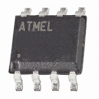
AT45DB041D-SSU Atmel, AT45DB041D-SSU Datasheet - Page 27

AT45DB041D-SSU
Manufacturer Part Number
AT45DB041D-SSU
Description
IC FLASH 4MBIT 66MHZ 8SOIC
Manufacturer
Atmel
Specifications of AT45DB041D-SSU
Format - Memory
FLASH
Memory Type
DataFLASH
Memory Size
4M (2048 pages x 264 bytes)
Speed
66MHz
Interface
SPI, RapidS
Voltage - Supply
2.7 V ~ 3.6 V
Operating Temperature
-40°C ~ 85°C
Package / Case
8-SOIC (3.9mm Width)
Density
4Mb
Access Time (max)
6ns
Interface Type
Serial (SPI)
Boot Type
Not Required
Address Bus
1b
Operating Supply Voltage (typ)
3/3.3V
Operating Temp Range
-40C to 85C
Package Type
SOIC
Program/erase Volt (typ)
2.7 to 3.6V
Sync/async
Synchronous
Operating Temperature Classification
Industrial
Operating Supply Voltage (min)
2.7V
Operating Supply Voltage (max)
3.6V
Supply Current
15mA
Mounting
Surface Mount
Pin Count
8
Architecture
Sectored
Supply Voltage (max)
3.6 V
Supply Voltage (min)
2.7 V
Maximum Operating Current
15 mA
Mounting Style
SMD/SMT
Organization
64 KB x 8
Memory Configuration
2048 Pages X 256 Bytes
Clock Frequency
50MHz
Supply Voltage Range
2.7V To 3.6V
Memory Case Style
SOIC
Rohs Compliant
Yes
Lead Free Status / RoHS Status
Lead free / RoHS Compliant
Available stocks
Company
Part Number
Manufacturer
Quantity
Price
Company:
Part Number:
AT45DB041D-SSU
Manufacturer:
ATMEL
Quantity:
12 000
Part Number:
AT45DB041D-SSU
Manufacturer:
ATMEL/爱特梅尔
Quantity:
20 000
Part Number:
AT45DB041D-SSU-2.5
Manufacturer:
ATMEL/爱特梅尔
Quantity:
20 000
14.2
3595P–DFLASH–09/09
Operation Mode Summary
The commands described previously can be grouped into four different categories to better
describe which commands can be executed at what times.
Group A commands consist of:
Group B commands consist of:
Group C commands consist of:
Group D commands consist of:
If a Group A command is in progress (not fully completed), then another command in Group A,
B, C, or D should not be started. However, during the internally self-timed portion of Group B
commands, any command in Group C can be executed. The Group B commands using buffer 1
should use Group C commands using buffer 2 and vice versa. Finally, during the internally self-
timed portion of a Group D command, only the Status Register Read command should be
executed.
1. Main Memory Page Read
2. Continuous Array Read
3. Read Sector Protection Register
4. Read Sector Lockdown Register
5. Read Security Register
1. Page Erase
2. Block Erase
3. Sector Erase
4. Chip Erase
5. Main Memory Page to Buffer 1 (or 2) Transfer
6. Main Memory Page to Buffer 1 (or 2) Compare
7. Buffer 1 (or 2) to Main Memory Page Program with Built-in Erase
8. Buffer 1 (or 2) to Main Memory Page Program without Built-in Erase
9. Main Memory Page Program through Buffer 1 (or 2)
10. Auto Page Rewrite
1. Buffer 1 (or 2) Read
2. Buffer 1 (or 2) Write
3. Status Register Read
4. Manufacturer and Device ID Read
1. Erase Sector Protection Register
2. Program Sector Protection Register
3. Sector Lockdown
4. Program Security Register
AT45DB041D
27


