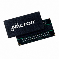
MT46H8M16LFCF-10 Micron Technology Inc, MT46H8M16LFCF-10 Datasheet - Page 14

MT46H8M16LFCF-10
Manufacturer Part Number
MT46H8M16LFCF-10
Description
IC DDR SDRAM 128MBIT 60VFBGA
Manufacturer
Micron Technology Inc
Type
DDR SDRAMr
Specifications of MT46H8M16LFCF-10
Format - Memory
RAM
Memory Type
Mobile DDR SDRAM
Memory Size
128M (8Mx16)
Speed
100MHz
Interface
Parallel
Voltage - Supply
1.7 V ~ 1.9 V
Operating Temperature
0°C ~ 70°C
Package / Case
60-VFBGA
Organization
8Mx16
Density
128Mb
Address Bus
15b
Access Time (max)
7ns
Maximum Clock Rate
104MHz
Operating Supply Voltage (typ)
1.8V
Package Type
VFBGA
Operating Temp Range
0C to 70C
Operating Supply Voltage (max)
1.9V
Operating Supply Voltage (min)
1.7V
Supply Current
90mA
Pin Count
60
Mounting
Surface Mount
Operating Temperature Classification
Commercial
Lead Free Status / RoHS Status
Lead free / RoHS Compliant
Available stocks
Company
Part Number
Manufacturer
Quantity
Price
Company:
Part Number:
MT46H8M16LFCF-10
Manufacturer:
Micron Technology Inc
Quantity:
10 000
Company:
Part Number:
MT46H8M16LFCF-10 IT
Manufacturer:
Micron Technology Inc
Quantity:
10 000
Company:
Part Number:
MT46H8M16LFCF-10 IT TR
Manufacturer:
Micron Technology Inc
Quantity:
10 000
Company:
Part Number:
MT46H8M16LFCF-10 TR
Manufacturer:
Micron Technology Inc
Quantity:
10 000
Stopping the External Clock
Figure 6:
PDF: 09005aef822b7e27/Source: 09005aef822b7dd6
MT46H8M16LFB_2.fm - Rev. A 5/06 EN
Clock Stop Mode
Notes:
1. Change the clock frequency, when the data transfers require a different rate of speed.
2. Stopping the clock altogether.
2. Any valid command is allowed, device is not in clock suspend mode.
3. Any DRAM operation already in process must be completed before entering clock stop
4. To enter and maintain a clock stop mode: CK = LOW, CK# = HIGH, CKE = HIGH.
One method of controlling the power efficiency in applications is to throttle the clock
which controls the SDRAM. There are two basic ways to control the clock:
Both of these are specific to the application and its requirements and both allow power
savings due to possible less transitions on the clock path.
The Mobile DDR SDRAM allows the clock to change frequency during operation, only if
all the timing parameters are met with respect to that change and all refresh require-
ments are satisfied.
The clock can also be stopped all together, if there are no data accesses in progress,
either WRITEs or READs that would be effected by this change; i.e., if a WRITE or a READ
is in progress the entire data burst must be through the pipeline prior to stopping the
clock. CKE must be held HIGH with CK = LOW and CK# = HIGH for the full duration of
the clock stop mode. One clock cycle and at least one NOP is required after the clock is
restarted before a valid command can be issued. Figure 6 on page 14 illustrates the clock
stop mode.
It is recommended that the Mobile DDR SDRAM should be in a precharged state if any
changes to the clock frequency are expected. This will eliminate timing violations that
may otherwise occur during normal operational accesses.
COMMAND
1. Prior to Ta1 the device is in clock stop mode. To exit, at least one NOP is required before any
DQ, DQS
Address
valid command.
mode. This includes
DRAM must be either in the idle or precharge state before clock suspend mode can be
entered.
CKE
CK#
CK
High-Z
Exit clock stop mode
(
(
(
(
(
(
)
(
)
(
)
)
)
)
)
)
(
(
(
(
(
(
)
(
)
(
)
)
)
)
)
)
t
RCD,
NOP
Ta1
t
1
RP,
14
t
RFC,
t
128Mb: 8 Meg x 16 Mobile DDR SDRAM
MRD,
CMD
Valid
Ta2
Micron Technology, Inc., reserves the right to change products or specifications without notice.
2
t
WR, all data-out for READ bursts. This means the
(
(
(
(
(
)
(
(
)
(
)
(
)
)
)
)
)
)
(
(
(
(
(
(
)
(
)
(
)
(
)
)
)
)
)
)
CMD
Tb3
Valid
2
All DRAM activities must be complete
Tb4
NOP
©2006 Micron Technology, Inc. All rights reserved.
Register Definition
Enter clock stop mode
NOP
DON’T CARE
Advance
(
(
(
(
)
(
(
)
(
)
(
)
)
)
)
)
4
(
(
(
(
(
3
(
)
(
)
(
)
)
)
)
)
)


