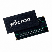
MT46H8M16LFCF-10 Micron Technology Inc, MT46H8M16LFCF-10 Datasheet - Page 48

MT46H8M16LFCF-10
Manufacturer Part Number
MT46H8M16LFCF-10
Description
IC DDR SDRAM 128MBIT 60VFBGA
Manufacturer
Micron Technology Inc
Type
DDR SDRAMr
Specifications of MT46H8M16LFCF-10
Format - Memory
RAM
Memory Type
Mobile DDR SDRAM
Memory Size
128M (8Mx16)
Speed
100MHz
Interface
Parallel
Voltage - Supply
1.7 V ~ 1.9 V
Operating Temperature
0°C ~ 70°C
Package / Case
60-VFBGA
Organization
8Mx16
Density
128Mb
Address Bus
15b
Access Time (max)
7ns
Maximum Clock Rate
104MHz
Operating Supply Voltage (typ)
1.8V
Package Type
VFBGA
Operating Temp Range
0C to 70C
Operating Supply Voltage (max)
1.9V
Operating Supply Voltage (min)
1.7V
Supply Current
90mA
Pin Count
60
Mounting
Surface Mount
Operating Temperature Classification
Commercial
Lead Free Status / RoHS Status
Lead free / RoHS Compliant
Available stocks
Company
Part Number
Manufacturer
Quantity
Price
Company:
Part Number:
MT46H8M16LFCF-10
Manufacturer:
Micron Technology Inc
Quantity:
10 000
Company:
Part Number:
MT46H8M16LFCF-10 IT
Manufacturer:
Micron Technology Inc
Quantity:
10 000
Company:
Part Number:
MT46H8M16LFCF-10 IT TR
Manufacturer:
Micron Technology Inc
Quantity:
10 000
Company:
Part Number:
MT46H8M16LFCF-10 TR
Manufacturer:
Micron Technology Inc
Quantity:
10 000
Table 14:
Table 15:
PDF: 09005aef822b7e27/Source: 09005aef822b7dd6
MT46H8M16LFB_2.fm - Rev. A 5/06 EN
Parameter
Delta input/output capacitance: DQs, DQS, DM
Delta input capacitance: Command and address
Delta input capacitance: CK, CK#
Input/output capacitance: DQs, DQS, DM
Input capacitance: Address
Input capacitance: Command
Input capacitance: CK, CK#
Parameter/Condition
Operating one bank active precharge current:
t
Address inputs are switching every two clock cycles; Data bus inputs
are stable
Operating current: One bank; Active-Read-Precharge; Burst = 4;
t
inputs changing once per clock cycle
Precharge power-down standby current: All banks idle; CKE is LOW; CS
is HIGH;
every two clock cycles; Data bus inputs are stable
Precharge power-down standby current with clock stopped: All banks
idle; CKE is LOW; CS is HIGH; CK = LOW, CK# = HIGH; Address and
control inputs are switching every two clock cycles; Data bus inputs
are stable
Precharge non power-down standby current: All banks idle;
CKE = HIGH; CS = HIGH;
are switching every two clock cycles; Data bus inputs are stable
Precharge non power-down standby current: Clock stopped; All banks
idle; CKE = HIGH; CS = HIGH; CK = LOW; CK# = HIGH Address and
control inputs are switching every two clock cycles; Data bus inputs
are stable
Active power-down standby current: One bank active; CKE = LOW;
CS = HIGH;
every two clock cycles; Data bus inputs are stable
Active power-down standby current: Clock stopped; One bank active;
CKE = LOW; CS = HIGH; CK = LOW; CK# = HIGH; Address and control
inputs are switching every two clock cycles; Data bus inputs are stable
Active non power-down standby: One bank active; CKE = HIGH;
CS = HIGH;
every two cycles; Data bus inputs are stable
Active non-power-down standby: Clock stopped; One bank active;
CKE = HIGH; CS = HIGH; CK = LOW; CK# = HIGH; Address and control
inputs are switching every two clock cycles; Data bus inputs are stable.
Operating burst read: One bank active; BL = 4;
Continuous read bursts; I
50% data changing each burst
CK =
RC =
t
t
RC (MIN);
CK (MIN); CKE is HIGH; CS is HIGH between valid commands;
t
CK =
t
t
CK =
CK =
Capacitance
Notes: 13; notes appear on pages 52–54
I
Notes: 1–5, 7, 10, 12, 14 notes appear on pages 52–54; V
DD
t
CK (MIN); Address and control inputs are switching
t
CK =
t
t
CK (MIN); Address and control inputs are switching
CK (MIN); Address and control inputs are switching
Specifications and Conditions
t
CK (MIN); I
t
CK =
OUT
= 0mA; Address inputs are switching;
t
CK (MIN); Address and control inputs
OUT
= 0mA; Address and control
t
t
RC =
CK =
t
t
RC (MIN);
CK (MIN);
48
Symbol
CDCK
CDIO
CCK
CIO
CDI
CI
CI
128Mb: 8 Meg x 16 Mobile DDR SDRAM
DD
Micron Technology, Inc., reserves the right to change products or specifications without notice.
Q = +1.8 ±0.1V, V
Symbol
I
I
I
I
I
DD
I
DD
I
I
DD
I
DD
DD
DD
I
I
DD
DD
DD
DD
DD
Min
TBD
TBD
TBD
TBD
TBD
TBD
TBD
2NS
3NS
2PS
3PS
2N
3N
4R
2P
3P
0
1
105
200
200
-75
80
25
15
25
20
95
3
3
Max
TBD
TBD
TBD
TBD
TBD
TBD
TBD
Max
Electrical Specifications
DD
= +1.8 ±0.1V
100
200
200
-10
75
25
15
25
20
90
©2006 Micron Technology, Inc. All rights reserved.
3
3
Units
pF
pF
pF
pF
pF
pF
pF
Units
mA
mA
mA
mA
mA
mA
mA
mA
mA
µA
µA
Notes
Notes
Advance
19, 36
19, 36
19, 36
21
26
26
35
35
19
19


