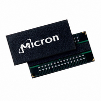
MT46H8M16LFCF-10 Micron Technology Inc, MT46H8M16LFCF-10 Datasheet - Page 8

MT46H8M16LFCF-10
Manufacturer Part Number
MT46H8M16LFCF-10
Description
IC DDR SDRAM 128MBIT 60VFBGA
Manufacturer
Micron Technology Inc
Type
DDR SDRAMr
Specifications of MT46H8M16LFCF-10
Format - Memory
RAM
Memory Type
Mobile DDR SDRAM
Memory Size
128M (8Mx16)
Speed
100MHz
Interface
Parallel
Voltage - Supply
1.7 V ~ 1.9 V
Operating Temperature
0°C ~ 70°C
Package / Case
60-VFBGA
Organization
8Mx16
Density
128Mb
Address Bus
15b
Access Time (max)
7ns
Maximum Clock Rate
104MHz
Operating Supply Voltage (typ)
1.8V
Package Type
VFBGA
Operating Temp Range
0C to 70C
Operating Supply Voltage (max)
1.9V
Operating Supply Voltage (min)
1.7V
Supply Current
90mA
Pin Count
60
Mounting
Surface Mount
Operating Temperature Classification
Commercial
Lead Free Status / RoHS Status
Lead free / RoHS Compliant
Available stocks
Company
Part Number
Manufacturer
Quantity
Price
Company:
Part Number:
MT46H8M16LFCF-10
Manufacturer:
Micron Technology Inc
Quantity:
10 000
Company:
Part Number:
MT46H8M16LFCF-10 IT
Manufacturer:
Micron Technology Inc
Quantity:
10 000
Company:
Part Number:
MT46H8M16LFCF-10 IT TR
Manufacturer:
Micron Technology Inc
Quantity:
10 000
Company:
Part Number:
MT46H8M16LFCF-10 TR
Manufacturer:
Micron Technology Inc
Quantity:
10 000
Functional Description
Initialization
PDF: 09005aef822b7e27/Source: 09005aef822b7dd6
MT46H8M16LFB_2.fm - Rev. A 5/06 EN
1. To prevent device latch-up, it is recommended the core power (V
2. Once power supply voltages are stable and the CKE has been driven HIGH, it is safe to
3. Once the clock is stable, a 200µs (minimum) delay is required by the Mobile DDR
4. Issue a PRECHARGE ALL command.
5. Issue NOP or DESELECT commands for at least
6. Issue an AUTO REFRESH command followed by NOP or DESELECT commands for at
The 128Mb Mobile DDR SDRAM is a high-speed CMOS, dynamic random-access
memory containing 134,217,728-bits. It is internally configured as a quad-bank DRAM.
Each of the 33,554,432-bit banks is organized as 4,096 rows by 512 columns by 16 bits.
The 128Mb Mobile DDR SDRAM uses a double data rate architecture to achieve high-
speed operation. The double data rate architecture is essentially a 2n-prefetch architec-
ture, with an interface designed to transfer two data words per clock cycle at the I/O
balls. single read or write access for the 128Mb Mobile DDR SDRAM consists of a single
2n-bit wide, one-clock-cycle data transfer at the internal DRAM core and two corre-
sponding n-bit wide, one-half-clock-cycle data transfers at the I/O balls.
Read and write accesses to the Mobile DDR SDRAM are burst oriented; accesses start at
a selected location and continue for a programmed number of locations in a
programmed sequence. Accesses begin with the registration of an ACTIVE command,
which is then followed by a READ or WRITE command. The address bits registered coin-
cident with the ACTIVE command are used to select the bank and row to be accessed
(BA0, BA1 select the bank; A0–A11 select the row). The address bits registered coincident
with the READ or WRITE command are used to select the starting column location for
the burst access.
It should be noted that the DLL signal that is typically used on standard DDR devices is
not necessary on the Mobile DDR SDRAM. It has been omitted to save power.
Prior to normal operation, the Mobile DDR SDRAM must be initialized. The following
sections provide detailed information covering device initialization, register definition,
command descriptions and device operation.
Mobile DDR SDRAMs must be powered up and initialized in a predefined manner.
Operational procedures other than those specified may result in undefined operation.
If there is an interruption to the device power, the initialization routine should be
followed to ensure proper functionality of the Mobile DDR SDRAM. The clock stop
feature is not available until the device has been properly initialized.
To properly initialize the Mobile DDR SDRAM, this sequence must be followed:
(V
power sources are used, V
apply the clock.
SDRAM prior to applying an executable command. During this time, NOP or DESE-
LECT commands must be issued on the command bus.
least
LECT commands for at least
AUTO REFRESH commands must be issued. Typically, both of these commands are
issued at this stage as described above. Alternately, the second AUTO REFRESH com-
mand and NOP or DESELECT sequence can be issued between steps 10 and 11.
DD
Q) be from the same power source and brought up simultaneously. If separate
t
RFC time. Issue a second AUTO REFRESH command followed by NOP or DESE-
DD
8
t
must lead V
RFC time. As part of the individualization sequence, two
128Mb: 8 Meg x 16 Mobile DDR SDRAM
Micron Technology, Inc., reserves the right to change products or specifications without notice.
DD
Q.
t
RP time.
Functional Description
©2006 Micron Technology, Inc. All rights reserved.
DD
) and I/O power
Advance


