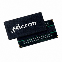
MT41J256M4HX-15E:D TR Micron Technology Inc, MT41J256M4HX-15E:D TR Datasheet - Page 40

MT41J256M4HX-15E:D TR
Manufacturer Part Number
MT41J256M4HX-15E:D TR
Description
IC DDR3 SDRAM 1GBIT 78FBGA
Manufacturer
Micron Technology Inc
Type
DDR3 SDRAMr
Specifications of MT41J256M4HX-15E:D TR
Format - Memory
RAM
Memory Type
DDR3 SDRAM
Memory Size
1G (256M x 4)
Speed
667MHz
Interface
Parallel
Voltage - Supply
1.425 V ~ 1.575 V
Operating Temperature
0°C ~ 95°C
Package / Case
78-FBGA
Organization
256Mx4
Density
1Gb
Address Bus
17b
Maximum Clock Rate
1.333GHz
Operating Supply Voltage (typ)
1.5V
Package Type
FBGA
Operating Temp Range
0C to 95C
Operating Supply Voltage (max)
1.575V
Operating Supply Voltage (min)
1.425V
Supply Current
220mA
Pin Count
78
Mounting
Surface Mount
Operating Temperature Classification
Commercial
Lead Free Status / RoHS Status
Lead free / RoHS Compliant
- Current page: 40 of 181
- Download datasheet (9Mb)
Electrical Specifications – DC and AC
DC Operating Conditions
Table 20:
Input Operating Conditions
Table 21:
PDF: 09005aef826aa906/Source: 09005aef82a357c3
1Gb_DDR3_3.fm - Rev. F 11/08 EN
Parameter/Condition
Parameter/Condition
Supply voltage
I/O supply voltage
Input leakage current
Any input 0V ≤ V
(All other pins not under test = 0V)
V
V
(All other pins not under test = 0V)
Input reference voltage command/address bus
I/O reference voltage DQ bus
Command/address termination voltage
(system level, not direct DRAM input)
REF
REF
DQ = V
supply leakage current
DD
DC Electrical Characteristics and Operating Conditions
All voltages are referenced to V
DC Electrical Characteristics and Input Conditions
All voltages are referenced to V
/2 or V
IN
Notes:
Notes:
≤ V
REF
DD
CA = V
, V
REF
1. V
2. V
3. V
4. The minimum limit requirement is for testing purposes. The leakage current on the V
1. V
2. DC values are determined to be less than 20 MHz in frequency. DRAM must meet specifica-
3. V
4. V
DD
pin 0V ≤ V
(0Hz to 250 kHz) specifications. V
parameters.
should be minimal.
Externally generated peak noise (noncommon mode) on V
× V
percent of V
tions if the DRAM induces additional AC noise greater than 20 MHz in frequency.
level. Externally generated peak noise (noncommon mode) on V
percent × V
exceed ±2 percent of V
tors. MIN and MAX values are system-dependent.
/2
DD
DD
REF
REF
REF
TT
DD
is not applied directly to the device. V
CA(
DQ(
and V
and V
(see Table 21).
around the V
DC
DC
IN
) is expected to be approximately 0.5 × V
DD
DD
) is expected to be approximately 0.5 × V
DD
≤ 1.1V
REF
Q must track one another. V
Q may include AC noise of ±50mV (250 kHz to 20 MHz) in addition to the DC
SS
SS
around the V
CA(
DC
V
V
REF
Symbol
REF
REF
).
Symbol
CA(
REF
V
DQ(
V
CA(
I
V
TT
VREF
DD
DQ(
DD
I
DC
I
DC
DC
Q
REF
) value. Peak-to-peak AC noise on V
40
)
)
DC
DQ(
).
DD
0.49 × V
0.49 × V
DC
and V
1.425
1.425
) value. Peak-to-peak AC noise on V
Min
Min
–2
–1
Micron Technology, Inc., reserves the right to change products or specifications without notice.
–
Electrical Specifications – DC and AC
DD
TT
DD
DD
DD
Q must be less than or equal to V
is a system supply for signal termination resis-
Q must be at same level for valid AC timing
0.5 × V
1Gb: x4, x8, x16 DDR3 SDRAM
0.5 × V
0.5 × V
Nom
DD
Nom
1.5
1.5
DD
–
–
and to track variations in the DC level.
and to track variations in the DC
DD
DD
DD
Q
REF
CA may not exceed ±1 percent
0.51 × V
0.51 × V
REF
©2006 Micron Technology, Inc. All rights reserved.
1.575
1.575
Max
REF
Max
2
1
CA should not exceed ±2
–
DQ may not exceed ±1
DD
DD
REF
Units
DQ should not
Units
DD
µA
µA
V
V
V
V
V
. V
SS
Notes
Notes
= V
REF
1, 2
1, 2
3, 4
1, 2
2, 3
4
SS
pin
Q.
Related parts for MT41J256M4HX-15E:D TR
Image
Part Number
Description
Manufacturer
Datasheet
Request
R

Part Number:
Description:
Manufacturer:
Micron Technology Inc
Datasheet:

Part Number:
Description:
Manufacturer:
Micron Technology Inc
Datasheet:

Part Number:
Description:
IC SDRAM 64MBIT 133MHZ 54TSOP
Manufacturer:
Micron Technology Inc
Datasheet:

Part Number:
Description:
IC SDRAM 64MBIT 5.5NS 86TSOP
Manufacturer:
Micron Technology Inc
Datasheet:

Part Number:
Description:
IC SDRAM 64MBIT 200MHZ 86TSOP
Manufacturer:
Micron Technology Inc
Datasheet:

Part Number:
Description:
IC SDRAM 64MBIT 133MHZ 54TSOP
Manufacturer:
Micron Technology Inc
Datasheet:

Part Number:
Description:
IC SDRAM 128MBIT 133MHZ 54TSOP
Manufacturer:
Micron Technology Inc
Datasheet:

Part Number:
Description:
IC SDRAM 256MBIT 133MHZ 90VFBGA
Manufacturer:
Micron Technology Inc
Datasheet:

Part Number:
Description:
IC SDRAM 128MBIT 133MHZ 54TSOP
Manufacturer:
Micron Technology Inc
Datasheet:

Part Number:
Description:
IC SDRAM 256MBIT 133MHZ 54TSOP
Manufacturer:
Micron Technology Inc
Datasheet:

Part Number:
Description:
IC DDR SDRAM 512MBIT 6NS 66TSOP
Manufacturer:
Micron Technology Inc
Datasheet:

Part Number:
Description:
IC SDRAM 128MBIT 167MHZ 86TSOP
Manufacturer:
Micron Technology Inc
Datasheet:

Part Number:
Description:
IC SDRAM 128MBIT 143MHZ 86TSOP
Manufacturer:
Micron Technology Inc
Datasheet:

Part Number:
Description:
SDRAM 256M-BIT 1.8V 54-PIN VFBGA
Manufacturer:
Micron Technology Inc
Datasheet:

Part Number:
Description:
IC SDRAM 128MBIT 143MHZ 86TSOP
Manufacturer:
Micron Technology Inc
Datasheet:


