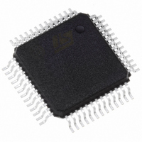
DSM2190F4V-15T6 STMicroelectronics, DSM2190F4V-15T6 Datasheet - Page 16

DSM2190F4V-15T6
Manufacturer Part Number
DSM2190F4V-15T6
Description
IC FLASH 2MBIT 150NS 52QFP
Manufacturer
STMicroelectronics
Datasheet
1.DSM2190F4V-15K6.pdf
(61 pages)
Specifications of DSM2190F4V-15T6
Format - Memory
FLASH
Memory Type
FLASH
Memory Size
2M (256K x 8)
Speed
150ns
Interface
Parallel
Voltage - Supply
3 V ~ 3.6 V
Operating Temperature
-40°C ~ 85°C
Package / Case
52-QFP
Operating Supply Voltage (typ)
3.3V
Operating Supply Voltage (min)
3V
Operating Supply Voltage (max)
3.6V
Operating Temp Range
-40C to 85C
Operating Temperature Classification
Industrial
Mounting
Surface Mount
Pin Count
52
Lead Free Status / RoHS Status
Lead free / RoHS Compliant
Other names
497-1323
Available stocks
Company
Part Number
Manufacturer
Quantity
Price
Company:
Part Number:
DSM2190F4V-15T6
Manufacturer:
STMicroelectronics
Quantity:
10 000
DSM2190F4
DETAILED OPERATION
Figure 5 shows major functional areas of the de-
vice:
The following describes these functions in more
detail.
Flash Memories
The Main Flash memory array is divided into eight
equal 32K byte sectors. The Secondary Flash
memory array is divided into four equal 8K byte
sectors. Each sector is selected by the DPLD can
be separately protected from program and erase
cycles. This configuration is specified by using PS-
Dsoft Express
Memory Sector Select Signals. The DPLD gen-
erates the Select signals for all the internal memo-
ry blocks (see Figure 14). Each of the twelve
sectors of the Flash memories has a select signal
( FS0-FS7, or CSBOOT0-CSBOOT3 ) which con-
tains up to three product terms. Having three prod-
uct terms for each select signal allows a given
sector to be mapped into multiple areas of system
memory if needed.
Ready/Busy (PC3). This signal can be used to
output the Ready/
output on Ready/
Flash memory array is being written, or when ei-
ther Flash memory array is being erased. The out-
put is a 1 (Ready) when no Write or Erase cycle is
16/61
Flash Memories
PLDs (DPLD, CPLD, Page Register)
DSP Bus Interface (Address, Data, Control)
I/O Ports
Runtime Control Registers
JTAG ISP Interface
TM
.
Busy
Busy
is a 0 (Busy) when either
status of the device. The
in progress. This signal may be polled by the DSP
or used as a DSP interrupt to indicate when an
erase or program cycle is complete.
Memory Operation. The Flash memories are ac-
cessed through the DSP Address, Data, and Con-
trol Bus Interface.
DSPs and MCUs cannot write to Flash memory as
it would an SRAM device. Flash memory must first
be “unlocked” with a special sequence of byte
write operations to invoke an internal algorithm,
then a single data byte is written to the Flash mem-
ory array, then programming status is checked by
a byte read operation or by checking the Ready/
Busy
struction sequences to program (write) data to the
Flash memory arrays, erase the arrays, and check
for different types of status from the arrays. These
instruction sequences are different combinations
of individual byte write and byte read operations.
IMPORTANT: The DSP may not read and execute
code from the same Flash memory array for which
it is directing an instruction sequence. Or more
simply stated, the DSP may not read code the
same Flash array that is writing or erasing. In-
stead, the DSP must execute code from an alter-
nate memory (like its own internal SRAM or a
different Flash array) while sending instructions to
a given Flash array. Since the two Flash memory
arrays inside the DSM device are completely inde-
pendent, the DSP may read code from one array
while sending instructions to the other.
After a Flash memory array is programmed (writ-
ten) it will go to “Read Array” mode, then the DSP
can read from Flash memory just as if would from
any 8-bit ROM or SRAM device.
pin (PC3). Table 5 lists all of the special in-


