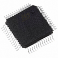
DSM2190F4V-15T6 STMicroelectronics, DSM2190F4V-15T6 Datasheet - Page 9

DSM2190F4V-15T6
Manufacturer Part Number
DSM2190F4V-15T6
Description
IC FLASH 2MBIT 150NS 52QFP
Manufacturer
STMicroelectronics
Datasheet
1.DSM2190F4V-15K6.pdf
(61 pages)
Specifications of DSM2190F4V-15T6
Format - Memory
FLASH
Memory Type
FLASH
Memory Size
2M (256K x 8)
Speed
150ns
Interface
Parallel
Voltage - Supply
3 V ~ 3.6 V
Operating Temperature
-40°C ~ 85°C
Package / Case
52-QFP
Operating Supply Voltage (typ)
3.3V
Operating Supply Voltage (min)
3V
Operating Supply Voltage (max)
3.6V
Operating Temp Range
-40C to 85C
Operating Temperature Classification
Industrial
Mounting
Surface Mount
Pin Count
52
Lead Free Status / RoHS Status
Lead free / RoHS Compliant
Other names
497-1323
Available stocks
Company
Part Number
Manufacturer
Quantity
Price
Company:
Part Number:
DSM2190F4V-15T6
Manufacturer:
STMicroelectronics
Quantity:
10 000
Table 3. Pin Description
ADIO0-15
CNTL0
CNTL1
CNTL2
Reset
PA0-7
PB0-7
PC0-7
PD0-2
V
GND
Pin Name
CC
In
In
In
In
In
I/O
I/O
I/O
I/O
Type
Sixteen address inputs from the DSP.
Active low write strobe input (WR) from the DSP
Active low read strobe input (RD) from the DSP.
Active low Byte Memory Select (BMS) signal from the DSP.
Active low reset input from system. Resets DSM I/O Ports, Page Register contents, and other
DSM configuration registers. Must be logic Low at Power-up.
Eight data bus signals connected to DSP pins D8 - D15.
Eight configurable Port B signals with the following functions:
Note: Each of the four Port B signals PB0-PB3 may be configured at run-time as either standard
Eight configurable Port C signals with the following functions:
Note 2: When used as general I/O, each of the eight Port C signals may be configured at run-time
Note 3: The JTAG ISP pins may be multiplexed with other I/O functions.
Three configurable Port D signals with the following functions:
Note 1: Port D pin PD0 (or any PLD input pin) can be connected to the DSP A16 output. See
Note 2: Port D pin PD1 (or any PLD input pin) can be connected to the DSP A17 output. See
Note 3: Port D pin PD2 (or any PLD input pin) can be connected to the DSP A18 output. See
Supply Voltage
Ground pins
Note 1: Port C pin PC2 input (or any PLD input pin) can be connected to the DSP IOMS output.
1. MCU I/O – DSP may write or read pins directly at runtime with csiop registers.
2. CPLD Output Macrocell (McellBC0-7) output.
3. Input to the PLDs (Input Macrocells).
4. Pins PC0, PC1, PC5, and PC6 can optionally form the JTAG IEEE-1149.1 ISP serial
5. Pins PC3 and PC4 can optionally form the enhanced JTAG signals TSTAT and TERR
6. Pin PC3 can optionally be configured as the Ready/Busy output to indicate Flash memory
1. MCU I/O – DSP may write or read pins directly at runtime with csiop registers.
2. CPLD Output Macrocell (McellAB0-7 or McellBC0-7) outputs.
3. Inputs to the PLDs (Input Macrocells).
1. MCU I/O – DSP may write or read pins directly at runtime with csiop registers.
2. Input to the PLDs (no associated Input Macrocells, routes directly into PLDs).
3. CPLD output (External Chip Select). Does not consume Output Macrocells.
4. Pin PD1 can optionally be configured as CLKIN, a common clock input to PLD.
5. Pin PD2 can optionally be configured as CSI, an active low Chip Select Input to select Flash
interface as signals TMS, TCK, TDI, and TDO respectively.
respectively. Reduces ISP programming time by up to 30% when used in addition to the
standard four JTAG signals: TDI, TDO, TMS, TCK.
programming status during parallel programming. May be polled by DSP or used as DSP
interrupt to indicate when Flash memory byte programming or erase operations are
complete.
memory. Flash memory is disabled to conserve more power when CSI is logic high. Can
connect CSI to ADSP-218X PWDACK output signal.
CMOS or for high slew rate. Each of the four Port B signals PB3-PB7 may be configured at
run-time as either standard CMOS or Open Drain Outputs.
See Figure 6.
Figure 6
Figure 6.
Figure 6
as either standard CMOS or Open Drain Outputs.
Description
DSM2190F4
9/61


