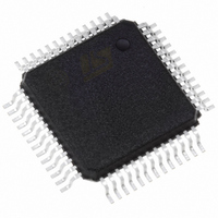
DSM2190F4V-15T6 STMicroelectronics, DSM2190F4V-15T6 Datasheet - Page 24

DSM2190F4V-15T6
Manufacturer Part Number
DSM2190F4V-15T6
Description
IC FLASH 2MBIT 150NS 52QFP
Manufacturer
STMicroelectronics
Datasheet
1.DSM2190F4V-15K6.pdf
(61 pages)
Specifications of DSM2190F4V-15T6
Format - Memory
FLASH
Memory Type
FLASH
Memory Size
2M (256K x 8)
Speed
150ns
Interface
Parallel
Voltage - Supply
3 V ~ 3.6 V
Operating Temperature
-40°C ~ 85°C
Package / Case
52-QFP
Operating Supply Voltage (typ)
3.3V
Operating Supply Voltage (min)
3V
Operating Supply Voltage (max)
3.6V
Operating Temp Range
-40C to 85C
Operating Temperature Classification
Industrial
Mounting
Surface Mount
Pin Count
52
Lead Free Status / RoHS Status
Lead free / RoHS Compliant
Other names
497-1323
Available stocks
Company
Part Number
Manufacturer
Quantity
Price
Company:
Part Number:
DSM2190F4V-15T6
Manufacturer:
STMicroelectronics
Quantity:
10 000
DSM2190F4
The DPLD performs address decoding, and gen-
erates select signals for internal and external com-
ponents, such as memory, registers, and I/O ports.
The DPLD can generates External Chip Select
(ECS0-ECS2) signals on Port D.
The CPLD can be used for logic functions, such as
loadable counters and shift registers, state ma-
chines, and encoding and decoding logic. These
logic functions can be constructed using the 16
Output Macrocells (OMC), 16 Input Macrocells
(IMC), and the AND Array.
The AND Array is used to form product terms.
These product terms are configured from the logic
definition entered in PSDsoft Express. An Input
Bus consisting of 64 signals is connected to the
PLDs. Input signals are shown in Table 9.
Figure 13. PLD Diagram
24/61
Data
Bus
64
64
16
16
8
3
Direct Macrocell Input to MCU Data Bus
Output Macrocell Feedback
DECODE PLD
REGISTER
Input Macrocell and Input Ports
(DPLD)
PAGE
CPLD
PORT D Inputs
ALLOC.
PT
8
4
1
3
1
16 Input Macrocell
(PORT B,C)
Macrocell
16 Output
Main Flash Memory Selects
Secondary Flash Memory Selects
External Chip Selects to Port D
CSIOP Select
JTAG Select
Turbo Bit. The PLDs in the device can minimize
power consumption by switching off when inputs
remain unchanged for an extended time of about
70 ns. Resetting the Turbo bit to 0 (Bit 3 of the
PMMR0 register) automatically places the PLDs
into standby if no inputs are changing. Turning the
Turbo mode off increases propagation delays
while reducing power consumption. Additionally,
five bits are available in the PMMR registers in
csiop to block DSP control signals from entering
the PLDs. This reduces power consumption and
can be used only when these DSP control signals
are not used in PLD logic equations. Each of the
two PLDs has unique characteristics suited for its
applications. They are described in the following
sections.
Direct Macrocell Access from MCU Data Bus
Macrocell
Alloc.
to PORT B or C
MCELLAB
MCELLBC
to PORT B
AI04957B
8
8


