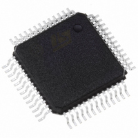
DSM2190F4V-15T6 STMicroelectronics, DSM2190F4V-15T6 Datasheet - Page 30

DSM2190F4V-15T6
Manufacturer Part Number
DSM2190F4V-15T6
Description
IC FLASH 2MBIT 150NS 52QFP
Manufacturer
STMicroelectronics
Datasheet
1.DSM2190F4V-15K6.pdf
(61 pages)
Specifications of DSM2190F4V-15T6
Format - Memory
FLASH
Memory Type
FLASH
Memory Size
2M (256K x 8)
Speed
150ns
Interface
Parallel
Voltage - Supply
3 V ~ 3.6 V
Operating Temperature
-40°C ~ 85°C
Package / Case
52-QFP
Operating Supply Voltage (typ)
3.3V
Operating Supply Voltage (min)
3V
Operating Supply Voltage (max)
3.6V
Operating Temp Range
-40C to 85C
Operating Temperature Classification
Industrial
Mounting
Surface Mount
Pin Count
52
Lead Free Status / RoHS Status
Lead free / RoHS Compliant
Other names
497-1323
Available stocks
Company
Part Number
Manufacturer
Quantity
Price
Company:
Part Number:
DSM2190F4V-15T6
Manufacturer:
STMicroelectronics
Quantity:
10 000
DSM2190F4
DSP Bus Interface
The “no-glue logic” DSP Bus Interface allows di-
rect connection. DSP address, data, and control
signals connect directly to the DSM device. See
Figure 6 for typical connections.
DSP address, data and control signals are routed
to Flash memory, I/O control ( csiop ), OMCs, and
IMCs within the DMS. The DSP address range for
each of these components is specified in PSDsoft
Express
I/O Ports
There are three programmable I/O ports: Ports B,
C, and D. Each of the ports is eight bits except Port
D, which is 3 bits. Each port pin is individually user
configurable, thus allowing multiple functions per
port. The ports are configured using PSDsoft Ex-
Figure 19. General I/O Port Architecture
As shown in Figure 19, the ports contain an output
multiplexer whose select signals are driven by the
configuration bits determined by PSDsoft Express.
Inputs to the multiplexer include the following:
30/61
Output data from the Data Out register (for MCU
I/O mode)
CPLD Macrocell output (OMC)
TM
.
EXT CS
Macrocell Outputs
WR
WR
ENABLE PRODUCT TERM ( .OE )
CPLD -INPUT
DATA OUT
READ MUX
DIR REG.
D
D
REG.
P
D
B
Q
Q
DATA IN
DATA OUT
press
in the csiop block.
The topics discussed in this section are:
General Port Architecture. The general archi-
tecture of the I/O Port block is shown in Figure 19.
Individual Port architectures are shown in Figure
20 to Figure 23. In general, once the purpose for a
port pin has been defined in PSDsoft Express
that pin is no longer available for other purposes.
Exceptions are noted.
The Port Data Buffer (PDB) is a tri-state buffer that
allows only one source at a time to be read by the
DSP. The Port Data Buffer (PDB) is connected to
the Internal Data Bus for feedback and can be
read by the DSP. The Data Out and Macrocell out-
General Port architecture
Port operating modes
Port Configuration Registers (PCR)
Port Data Registers
Individual Port functionality.
External Chip Selects ESC0-2 from the DPLD to
Port D pins only.
TM
or by the DSP writing to on-chip registers
OUTPUT
OUTPUT
SELECT
MUX
ENABLE OUT
Macrocell
Input
PORT PIN
AI04905B
TM
,


