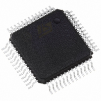
DSM2190F4V-15T6 STMicroelectronics, DSM2190F4V-15T6 Datasheet - Page 6

DSM2190F4V-15T6
Manufacturer Part Number
DSM2190F4V-15T6
Description
IC FLASH 2MBIT 150NS 52QFP
Manufacturer
STMicroelectronics
Datasheet
1.DSM2190F4V-15K6.pdf
(61 pages)
Specifications of DSM2190F4V-15T6
Format - Memory
FLASH
Memory Type
FLASH
Memory Size
2M (256K x 8)
Speed
150ns
Interface
Parallel
Voltage - Supply
3 V ~ 3.6 V
Operating Temperature
-40°C ~ 85°C
Package / Case
52-QFP
Operating Supply Voltage (typ)
3.3V
Operating Supply Voltage (min)
3V
Operating Supply Voltage (max)
3.6V
Operating Temp Range
-40C to 85C
Operating Temperature Classification
Industrial
Mounting
Surface Mount
Pin Count
52
Lead Free Status / RoHS Status
Lead free / RoHS Compliant
Other names
497-1323
Available stocks
Company
Part Number
Manufacturer
Quantity
Price
Company:
Part Number:
DSM2190F4V-15T6
Manufacturer:
STMicroelectronics
Quantity:
10 000
DSM2190F4
ARCHITECTURAL OVERVIEW
Major functional blocks are shown in Figure 5.
DSP Address/Data/Control Interface
These DSP signals attach directly to the DSM for
a glueless connection. An 8-bit data connection is
formed and all 22 DSP address lines can be de-
coded as well as DSP memory strobes;
IOMS
DSM2190F4 can be configured and used depend-
ing on system requirements. One convenient way
is to combine the function of the
the
access DSM memory at runtime even after the
boot process is complete using only the
nal. Combining
pin(s) on the DMS device. See Analog Devices
ADSP-2191 DSP Hardware Reference Manual,
Chapter 7, Code Example: BMS Runtime Access.
Alternatively, any of the
used to decode any of the sectors of DSM Main
Flash or Secondary flash memories.
Main Flash Memory
The 2M bit (256K x 8) Flash memory is divided into
eight equally-sized 32K byte sectors that are indi-
vidually selectable through the Decode PLD. Each
Flash memory sector can be located at any ad-
dress as defined by the user with PSDsoft Ex-
press. DSP code and data is easily placed in flash
memory using the PSDsoft Express software de-
velopment tool.
Secondary Flash Memory
The 256K bit (32K x 8) Flash memory is divided
into eight equally-sized 8K byte sectors that are in-
dividually selectable through the Decode PLD.
Each Flash memory sector can be located at any
address as defined by the user with PSDsoft Ex-
press. DSP code and data can also be placed
Secondary Flash memory using the PSDsoft Ex-
press development tool.
Secondary flash memory is good for storing data
because of its small sectors. Additionally, software
EEPROM emulation techniques can be used for
small data sets that change frequently on a byte-
by-byte basis.
Secondary flash may also be used to store custom
start-up code for applications that do not “boot” us-
ing DMA, but instead start executing code from ex-
ternal memory upon reset. Storing code here can
keep the entire Main Flash free of initialization
code for clean software partitioning. If only one or
more 8K byte sectors are needed for start-up
code, the remaining sectors of Secondary Flash
may be used for data storage.
6/61
BMS
, and
signal. Doing this allows the DSP core to
MSx
. There are many different ways the
MSx
and
MSx
BMS
signals may also be
consumes less I/O
MSx
signals into
BMS
BMS
sig-
,
Secondary Flash may also be used as an exten-
sion to Main Flash memory producing a total of
288K bytes
Miscellaneous: Main and Secondary Flash memo-
ries are totally independent, allowing concurrent
operation if needed. The DSP can read from one
memory while erasing or programming the other.
The DSP can erase Flash memories by individual
sectors or the entire Flash memory array may be
erased at one time. Each sector in either Flash
memory may be individually write protected, block-
ing any writes from the DSP (good for boot and
start-up code protection). The Flash memories au-
tomatically go to standby between DSP read or
write accesses to conserve power. Maximum ac-
cess times include sector decoding time. Maxi-
mum erase cycles is 100K and data retention is 15
years minimum. Flash memory, as well as the en-
tire DSM device may be programmed with the
JTAG ISP interface with no DSP involvement.
Programmable Logic (PLDs)
The DSM family contains two PLDS that may op-
tionally run in Turbo or Non-Turbo mode. PLDs op-
erate faster (less propagation delay) while in
Turbo mode but consume more power than Non-
Turbo mode. Non-Turbo mode allows the PLDs to
automatically go to standby when no inputs are
change to conserve power. The Turbo mode set-
ting is controlled at runtime by DSP software.
Decode PLD (DPLD). This is programmable log-
ic used to select one of the eight individual Main
Flash memory segments, one of four individual
Secondary Flash memory segments, or the group
of control registers within the DSM device. The
DPLD can also optionally drive external chip select
signals on Port D pins. DPLD input signals include:
DSP address and control signals, Page Register
outputs, DSM Port Pins, CPLD logic feedback.
Complex PLD (CPLD). This programmable logic
is used to create both combinatorial and sequen-
tial general purpose logic. The CPLD contains 16
Output Macrocells (OMCs) and 16 Input Macro-
cells (IMCs). PSD Macrocell registers are unique
in that that have direct connection to the DSP data
bus allowing them to be loaded and read directly
by the DSP at runtime. This direct access is good
for making small peripheral devices (shifters,
counters, state machines, etc.) that are accessed
directly by the DSP with little overhead. DPLD in-
puts include DSP address and control signals,
Page Register outputs, DSM Port Pins, and CPLD
feedback.


