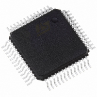
PSD813F1A-90MI STMicroelectronics, PSD813F1A-90MI Datasheet - Page 12

PSD813F1A-90MI
Manufacturer Part Number
PSD813F1A-90MI
Description
IC FLASH 1MBIT 90NS 52QFP
Manufacturer
STMicroelectronics
Datasheet
1.PSD813F1A-90U.pdf
(111 pages)
Specifications of PSD813F1A-90MI
Format - Memory
FLASH
Memory Type
FLASH
Memory Size
1M (128K x 8)
Speed
90ns
Interface
Parallel
Voltage - Supply
4.5 V ~ 5.5 V
Operating Temperature
-40°C ~ 85°C
Package / Case
52-QFP
Lead Free Status / RoHS Status
Lead free / RoHS Compliant
Other names
497-1978
Available stocks
Company
Part Number
Manufacturer
Quantity
Price
Company:
Part Number:
PSD813F1A-90MI
Manufacturer:
STMicroelectronics
Quantity:
10 000
PSD813F1A
Note: 1. The pin numbers in this table are for the PLCC package only. See the
12/111
Pin Name
GND
PC5
PC6
PC7
PD0
PD1
PD2
V
2. These functions can be multiplexed with other functions.
CC
13
12
11
10
9
8
15, 38
1, 16,
26
Pin
Type
I/O
I/O
I/O
I/O
I/O
I/O
PC5 pin of Port C. This port pin can be configured to have the following functions:
1. MCU I/O – write to or read from a standard output or input port.
2. CPLD macrocell (McellBC5) output.
3. Input to the PLDs.
4. TDI input
This pin can be configured as a CMOS or Open Drain output.
PC6 pin of Port C. This port pin can be configured to have the following functions:
1. MCU I/O – write to or read from a standard output or input port.
2. CPLD macrocell (McellBC6) output.
3. Input to the PLDs.
4. TDO output
This pin can be configured as a CMOS or Open Drain output.
PC7 pin of Port C. This port pin can be configured to have the following functions:
1. MCU I/O – write to or read from a standard output or input port.
2. CPLD macrocell (McellBC7) output.
3. Input to the PLDs.
4. DBE – active Low Data Byte Enable input from 68HC912 type MCUs.
This pin can be configured as a CMOS or Open Drain output.
PD0 pin of Port D. This port pin can be configured to have the following functions:
1. ALE/AS input latches address output from the MCU.
2. MCU I/O – write or read from a standard output or input port.
3. Input to the PLDs.
4. CPLD output (External Chip Select).
PD1 pin of Port D. This port pin can be configured to have the following functions:
1. MCU I/O – write to or read from a standard output or input port.
2. Input to the PLDs.
3. CPLD output (External Chip Select).
4. CLKIN – clock input to the CPLD macrocells, the APD Unit’s Power-down counter, and
the CPLD AND Array.
PD2 pin of Port D. This port pin can be configured to have the following functions:
1. MCU I/O – write to or read from a standard output or input port.
2. Input to the PLDs.
3. CPLD output (External Chip Select).
4. PSD Chip Select Input (CSI). When Low, the MCU can access the PSD memory and I/
O. When High, the PSD memory blocks are disabled to conserve power.
Supply Voltage
Ground pins
2
for the JTAG Interface.
2
for the JTAG Interface.
Description
Figure 2., page
(1)
7, for pin numbers on other package type.


