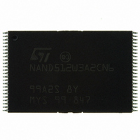
NAND512W3A2CN6E NUMONYX, NAND512W3A2CN6E Datasheet - Page 35

NAND512W3A2CN6E
Manufacturer Part Number
NAND512W3A2CN6E
Description
IC FLASH 512MBIT 48TSOP
Manufacturer
NUMONYX
Datasheet
1.NAND512R3A2CZA6E.pdf
(55 pages)
Specifications of NAND512W3A2CN6E
Format - Memory
FLASH
Memory Type
FLASH - Nand
Memory Size
512M (64M x 8)
Interface
Parallel
Voltage - Supply
2.7 V ~ 3.6 V
Operating Temperature
-40°C ~ 85°C
Package / Case
48-TSOP
Cell Type
NAND
Density
512Mb
Access Time (max)
12us
Interface Type
Parallel
Boot Type
Not Required
Address Bus
26b
Operating Supply Voltage (typ)
3/3.3V
Operating Temp Range
-40C to 85C
Package Type
TSOP
Program/erase Volt (typ)
2.7 to 3.6V
Sync/async
Asynchronous
Operating Temperature Classification
Industrial
Operating Supply Voltage (min)
2.7V
Operating Supply Voltage (max)
3.6V
Word Size
8b
Number Of Words
64M
Supply Current
20mA
Mounting
Surface Mount
Pin Count
48
Lead Free Status / RoHS Status
Lead free / RoHS Compliant
Speed
-
Lead Free Status / RoHS Status
Lead free / RoHS Compliant, Compliant
Available stocks
Company
Part Number
Manufacturer
Quantity
Price
Company:
Part Number:
NAND512W3A2CN6E
Manufacturer:
MICRON
Quantity:
1 500
Part Number:
NAND512W3A2CN6E
Manufacturer:
ST
Quantity:
20 000
NAND512-A2C
10
DC and AC parameters
This section summarizes the operating and measurement conditions, and the DC and AC
characteristics of the device. The parameters in the DC and AC characteristics tables that
follow, are derived from tests performed under the measurement conditions summarized in
Table 16: Operating and AC measurement
operating conditions in their circuit match the measurement conditions when relying on the
quoted parameters.
Table 16.
Table 17.
1. T
2. Input/output capacitances double on stacked devices.
Supply voltage (V
Ambient temperature (T
Load capacitance (C
and C
Input pulses voltages
Input and output timing ref. voltages
Input rise and fall times
Output circuit resistors, R
Symbol
C
C
A
I/O
IN
= 25 °C, f = 1 MHz. C
L
)
Input capacitance
Input/output
capacitance
Operating and AC measurement conditions
Capacitance
DD
Parameter
)
L
) (1 TTL GATE
A
)
IN
ref
Parameter
and C
(1)(2)
I/O
are not 100% tested.
Test conditions
V
V
1.8 V devices
1.8 V devices
1.8 V devices
1.8 V devices
3 V devices
3 V devices
3 V devices
3 V devices
IN
IL
conditions. Designers should check that the
Grade 6
= 0 V
= 0 V
Typ
Min
–40
1.7
2.7
0.4
0
NAND flash
8.35
DC and AC parameters
0.9
1.5
30
50
5
Max
Max
1.95
10
10
V
3.6
2.4
85
DD
Units
Unit
kΩ
pF
pF
°C
pF
pF
ns
V
V
V
V
V
V
35/55


