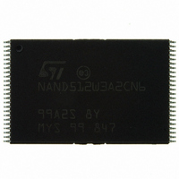
NAND512W3A2CN6E NUMONYX, NAND512W3A2CN6E Datasheet - Page 38

NAND512W3A2CN6E
Manufacturer Part Number
NAND512W3A2CN6E
Description
IC FLASH 512MBIT 48TSOP
Manufacturer
NUMONYX
Datasheet
1.NAND512R3A2CZA6E.pdf
(55 pages)
Specifications of NAND512W3A2CN6E
Format - Memory
FLASH
Memory Type
FLASH - Nand
Memory Size
512M (64M x 8)
Interface
Parallel
Voltage - Supply
2.7 V ~ 3.6 V
Operating Temperature
-40°C ~ 85°C
Package / Case
48-TSOP
Cell Type
NAND
Density
512Mb
Access Time (max)
12us
Interface Type
Parallel
Boot Type
Not Required
Address Bus
26b
Operating Supply Voltage (typ)
3/3.3V
Operating Temp Range
-40C to 85C
Package Type
TSOP
Program/erase Volt (typ)
2.7 to 3.6V
Sync/async
Asynchronous
Operating Temperature Classification
Industrial
Operating Supply Voltage (min)
2.7V
Operating Supply Voltage (max)
3.6V
Word Size
8b
Number Of Words
64M
Supply Current
20mA
Mounting
Surface Mount
Pin Count
48
Lead Free Status / RoHS Status
Lead free / RoHS Compliant
Speed
-
Lead Free Status / RoHS Status
Lead free / RoHS Compliant, Compliant
Available stocks
Company
Part Number
Manufacturer
Quantity
Price
Company:
Part Number:
NAND512W3A2CN6E
Manufacturer:
MICRON
Quantity:
1 500
Part Number:
NAND512W3A2CN6E
Manufacturer:
ST
Quantity:
20 000
DC and AC parameters
Table 21.
1. ES = electronic signature.
2. During a program/erase enable operation, t
38/55
Symbol
t
t
t
VLWH
t
t
t
t
t
t
t
ALLRL1
ALLRL2
t
t
t
t
t
t
t
t
t
t
t
BLBH1
BLBH2
BLBH3
BLBH4
t
t
CLLRL
WHBH
VHWH
RHQX
WHBL
WHRL
EHQZ
RHQZ
EHQX
BHRL
DZRL
ELQV
RHRL
RLRH
RLQV
RLRL
operation, t
(2)
symbol
t
t
t
PROG
VLWH
BERS
t
t
t
t
t
t
t
T
t
WHR
Alt.
t
AC characteristics for operations
t
t
REH
t
t
RST
CLR
CHZ
CEA
RHZ
REA
WW
t
WB
AR
RR
RP
RC
t
OH
IR
R
is the delay from WP Low to W High.
Address Latch Low to
Read Enable Low
Ready/Busy High to Read Enable Low
Ready/Busy Low to
Ready/Busy High
Command Latch Low to Read Enable Low
Data Hi-Z to Read Enable Low
Chip Enable High to Output Hi-Z
Chip Enable Low to Output Valid
Read Enable High to
Read Enable Low
Read Enable High to Output Hi-Z
Chip Enable High or Read Enable High to Output Hold
Read Enable Low to
Read Enable High
Read Enable Low to
Read Enable Low
Read Enable Low to
Output Valid
Write Enable High to
Ready/Busy High
Write Enable High to Ready/Busy Low
Write Enable High to Read Enable Low
Write protection time
VHWH
Read electronic signature
Read cycle
Read busy time
Program busy time
Erase busy time
Reset busy time, during ready
Reset busy time, during read
Reset busy time, during program
Reset busy time, during erase
Read Enable High hold time
Read Enable pulse width
Read cycle time
Read Enable access time
Read ES access time
Read busy time
is the delay from WP High to W High. During a program/erase disable
Parameter
(1)
Max
Max
Max
Max
Max
Max
Max
Max
Max
Max
Max
Max
Max
Min
Min
Min
Min
Min
Min
Min
Min
Min
Min
Min
devices
1.8 V
500
500
100
100
10
10
20
15
10
10
30
45
15
30
10
25
50
30
15
60
3
5
5
0
NAND512-A2C
devices
500
500
100
100
3 V
10
10
20
12
10
10
30
35
10
30
10
15
30
18
12
60
3
5
5
0
Unit
ms
ns
ns
ns
µs
µs
µs
µs
µs
µs
ns
ns
ns
ns
ns
ns
ns
ns
ns
ns
µs
ns
ns
ns


