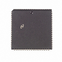
DP8421AV-25 National Semiconductor, DP8421AV-25 Datasheet - Page 28

DP8421AV-25
Manufacturer Part Number
DP8421AV-25
Description
IC CTRLR/DVR CMOS PROGRAM 68PLCC
Manufacturer
National Semiconductor
Datasheet
1.DP8420AV-25.pdf
(58 pages)
Specifications of DP8421AV-25
Controller Type
Dynamic RAM (DRAM)
Voltage - Supply
4.5 V ~ 5.5 V
Operating Temperature
0°C ~ 70°C
Package / Case
68-PLCC
Lead Free Status / RoHS Status
Contains lead / RoHS non-compliant
Other names
*DP8421AV-25
Available stocks
Company
Part Number
Manufacturer
Quantity
Price
Company:
Part Number:
DP8421AV-25
Manufacturer:
Texas Instruments
Quantity:
10 000
Part Number:
DP8421AV-25
Manufacturer:
NS/国半
Quantity:
20 000
5 0 Refresh Options
5 5 CLEARING THE REFRESH REQUEST CLOCK
The refresh request clock can be cleared by negating
DISRFSH and asserting RFSH for 500 ns one period of the
internal 2 MHz clock as shown in Figure 21 By clearing the
6 0 Port A Wait State Support
Wait states allow a CPU’s access cycle to be increased by
one or multiple CPU clock periods The wait or ready input is
named differently by CPU manufacturers However any
CPU’s wait or ready input is compatible with either the WAIT
or DTACK output of the DP8420A 21A 22A The user de-
termines whether to program WAIT or DTACK (R7) and
which value to select for WAIT or DTACK (R2 R3) depend-
ing upon the CPU used and where the CPU samples its wait
input during an access cycle
The decision to terminate the CPU access cycle is directly
affected by the speed of the DRAMs used The system de-
signer must ensure that the data from the DRAMs will be
present for the CPU to sample or that the data has been
written to the DRAM before allowing the CPU access cycle
to terminate
The insertion of wait states also allows a CPU’s access cy-
cle to be extended until the DRAM access has taken place
The DP8420A 21A 22A insert wait states into CPU access
cycles due to guaranteeing precharge time refresh current-
ly in progress user programmed wait states the WAITIN
signal being asserted and GRANTB not being valid
(DP8422A only) If one of these events is taking place and
the CPU starts an access the DP8420A 21A 22A will insert
wait states into the access cycle thereby increasing the
FIGURE 21 Clearing the Refresh Request Clock Counter
(Continued)
FIGURE 22 WAIT Type Output
28
22 Once WAIT is sampled negated the access cycle is
refresh request clock the user is guaranteed that an inter-
nal refresh request will not be generated for approximately
15 s one refresh clock period from the time RFSH is neg-
ated This action will also clear the refresh address counter
length of the CPU’s access Once the event has been com-
pleted the DP8420A 21A 22A will allow the access to take
place and stop inserting wait states
There are six programming bits R2 – R7 an input WAITIN
and an output that functions as WAIT or DTACK
6 1 WAIT TYPE OUTPUT
With the R7 address bit negated during programming the
user selects the WAIT output As long as WAIT is sampled
asserted by the CPU wait states (extra clock periods) are
inserted into the current access cycle as shown in Figure
completed by the CPU WAIT is asserted at the beginning of
a chip selected access and is programmed to negate a
number of positive edges and or negative levels of CLK
from the event that starts the access WAIT can also be
programmed to function in page burst mode applications
Once WAIT is negated during an access and the ECAS
inputs are negated with AREQ asserted WAIT can be pro-
grammed to toggle following the ECAS inputs Once AREQ
is negated ending the access WAIT will stay negated until
the next chip selected access For more details about WAIT
Type Output see Application Note AN-773
TL F 8588– 75
TL F 8588– 76


