ISL6296ADRTZ-T Intersil, ISL6296ADRTZ-T Datasheet - Page 14

ISL6296ADRTZ-T
Manufacturer Part Number
ISL6296ADRTZ-T
Description
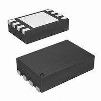
IC AUTHENTICATION DEVICE 8-TDFN
Manufacturer
Intersil
Series
FlexiHash™r
Datasheet
1.ISL6296ADHZ-T.pdf
(20 pages)
Specifications of ISL6296ADRTZ-T
Function
Battery Authentication
Battery Type
Li-Ion, Li-Pol, NiMH
Voltage - Supply
2.6 V ~ 4.8 V
Operating Temperature
-25°C ~ 85°C
Mounting Type
Surface Mount
Package / Case
8-TDFN Exposed Pad
Lead Free Status / RoHS Status
Lead free / RoHS Compliant
Available stocks
Company
Part Number
Manufacturer
Quantity
Price
Company:
Part Number:
ISL6296ADRTZ-T
Manufacturer:
INTERSIL
Quantity:
1 000
Company:
Part Number:
ISL6296ADRTZ-TR5302
Manufacturer:
RENESAS
Quantity:
32 462
Part Number:
ISL6296ADRTZ-TR5302
Manufacturer:
INTERSIL
Quantity:
20 000
Analog Biasing Components and Clock
Generation
The analog section in the ISL6296A mainly includes the
Time Base Generator and the internal regulator for powering
the circuits in the ISL6296A.
TIME BASE GENERATOR
A time base generator is included on-chip to provide timing
reference for serial data encoding and decoding at the XSD
bus interface. This eliminates the need for an external
crystal. The time base oscillator is trimmed during
manufacturing to a nominal frequency of 532.5kHz. It has a
frequency tolerance better than 5% over operating supply
voltage and temperature range.
INTERNAL VOLTAGE REGULATOR
The ISL6296A incorporates an internal voltage regulator that
maintains a nominal operating voltage of 2.5V within the
device. The regulator draws power directly from the VDD
input. No external component is required to regulate circuit
voltage. The regulator is shut off during Sleep mode.
Memory/Operational Register Description
The ISL6296A memory and register structure is organized
into 4 banks of 256 addressable locations. However, not all
NOTE: Information stored in address 0-0E (INF1) and 0-0F (INF2) is for use by the host firmware only. Actual content depends on the host firmware
customization preference.
ADDRESS
0-0C
0-0D
0-00
0-01
0-02
0-03
0-04
0-05
0-06
0-07
0-08
0-09
0-0A
0-0B
0-0E
0-0F
NAME
DTRM
DCFG
SE1C
SE1D
SE2C
SE2D
SE3C
SE3D
SE1A
SE1B
SE2A
SE2B
SE3A
SE3B
INF1
INF2
14
Default Configuration
Default Trimming
General Purpose
General Purpose
Auth Secret #1A
Auth Secret #1B
Auth Secret #1C
Auth Secret #1D
Auth Secret #2A
Auth Secret #2B
Auth Secret #2C
Auth Secret #2D
Auth Secret #3A
Auth Secret #3B
Auth Secret #3C
Auth Secret #3D
DESCRIPTION
TABLE 8. OTP ROM MEMORY MAP (BANK 0)
General purpose non-volatile memory for storage of model ID, date code, and other
cell information
BIT 7
HSF
ISL6296A
DAB[1:0]
BIT 6
of the addressable registers are used nor implemented.
Accessing a non-implemented register will result in the
access instruction being ignored. A bus error indication may
or may not be flagged.
Bank 0 is dedicated for the OTP ROM. There are 16 memory
locations implemented in the array. Writing to the OTP ROM
has no immediate effect on the chip operation until a
Power-on Reset occurred, or a soft reset is issued. Table 8
describes the OTP ROM memory assignment. The default
factory setting for address [0:00] is given in Table 11.
Bank 1 contains the Control and Status registers. Only 2
registers are implemented. Table 9 shows the register map
of the Bank 1 registers. Detailed descriptions of register
settings are given in Tables 14 and 15.
Bank 2 contains the Authentication registers. Only 3
registers are implemented. These registers are used during
the battery pack authentication process. Table 10 describes
the mapping of the Authentication registers.
Bank 3 is reserved for Intersil production testing only, and
will not be accessible during normal operation. Accessing
the Test and Trim Registers when not in test mode will result
in a bus error.
TIBB[2:0]
BIT 5
SPD[1:0]
BIT 4
S1C[7:0]
S1D[7:0]
S2C[7:0]
S2D[7:0]
S3C[7:0]
S3D[7:0]
S1A[7:0]
S1B[7:0]
S2A[7:0]
S2B[7:0]
S3A[7:0]
S3B[7:0]
BIT3
eINT
BIT 2
ASLP
TOSC[3:0]
BIT 1
SLO[1:0]
April 15, 2010
BIT 0
FN6567.3


