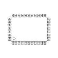
PCA8534AH/Q900/1,5 NXP Semiconductors, PCA8534AH/Q900/1,5 Datasheet - Page 18

PCA8534AH/Q900/1,5
Manufacturer Part Number
PCA8534AH/Q900/1,5
Description
IC LCD DRIVER 60SEG 80LQFP
Manufacturer
NXP Semiconductors
Datasheet
1.PCA8534AHQ90015.pdf
(44 pages)
Specifications of PCA8534AH/Q900/1,5
Package / Case
80-LQFP
Display Type
LCD
Configuration
60 Segment
Interface
I²C
Current - Supply
80µA
Voltage - Supply
1.8 V ~ 5.5 V
Operating Temperature
-40°C ~ 85°C
Mounting Type
Surface Mount
Number Of Digits
30
Number Of Segments
60
Maximum Clock Frequency
3046 Hz
Operating Supply Voltage
1.8 V to 5.5 V
Maximum Power Dissipation
400 mW
Maximum Operating Temperature
+ 95 C
Attached Touch Screen
No
Maximum Supply Current
20 uA
Minimum Operating Temperature
- 40 C
Lead Free Status / RoHS Status
Lead free / RoHS Compliant
Digits Or Characters
-
Lead Free Status / Rohs Status
Details
Other names
568-5110-2
Available stocks
Company
Part Number
Manufacturer
Quantity
Price
Company:
Part Number:
PCA8534AH/Q900/1,5
Manufacturer:
NXP Semiconductors
Quantity:
10 000
NXP Semiconductors
PCA8534A_2
Product data sheet
7.13 Output bank selector
7.14 Input bank selector
7.15 Blinker
This last step is very important because during writing data to the first PCA8534A, the
data pointer of the second PCA8534A is incremented. In addition, the hardware
subaddress should not be changed whilst the device is being accessed on the I
interface.
The output bank selector (see
address for transfer to the display register. The actual row selected depends on the LCD
drive mode in operation and on the instant in the multiplex sequence.
The SYNC signal resets these sequences to the following starting points: row 3 for
1:4 multiplex, row 2 for 1:3 multiplex, row 1 for 1:2 multiplex and row 0 for static mode.
The PCA8534A includes a RAM bank switching feature in the static and 1:2 multiplex
drive modes. In static drive mode, the bank-select command may request the contents of
row 2 to be selected for display instead of the contents of row 0. In 1:2 multiplex drive
mode, the contents of rows 2 and 3 may be selected instead of rows 0 and 1. This
enables preparation of display information in an alternative bank and the ability to switch
to it once it has been assembled.
The input bank selector loads display data into the display RAM in accordance with the
selected LCD drive configuration. Display data can be loaded in row 2 in static drive mode
or in rows 2 and 3 in 1:2 multiplex drive mode by using the bank-select command. The
input bank selector functions independently to the output bank selector.
The display blinking capabilities of the PCA8534A are very versatile. The whole display
can be blinked at frequencies set by the blink-select command (see
blinking frequencies are fractions of the clock frequency. The ratios between the clock and
blinking frequencies depend on the mode in which the device is operating (see
•
•
•
•
In 1:4 multiplex mode: all RAM addresses of row 0 are selected, followed sequentially
by the contents of row 1, row 2, and then row 3.
In 1:3 multiplex mode: rows 0, 1, and 2 are selected sequentially.
In 1:2 multiplex mode: rows 0 and 1 are selected.
In the static mode: row 0 is selected.
All information provided in this document is subject to legal disclaimers.
Rev. 02 — 1 June 2010
Table
14), selects one of the four rows per display RAM
Universal LCD driver for low multiplex rates
PCA8534A
Table
© NXP B.V. 2010. All rights reserved.
15). The
Table
2
C-bus
18 of 44
7).


