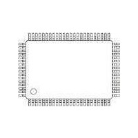
PCA8534AH/Q900/1,5 NXP Semiconductors, PCA8534AH/Q900/1,5 Datasheet - Page 19

PCA8534AH/Q900/1,5
Manufacturer Part Number
PCA8534AH/Q900/1,5
Description
IC LCD DRIVER 60SEG 80LQFP
Manufacturer
NXP Semiconductors
Datasheet
1.PCA8534AHQ90015.pdf
(44 pages)
Specifications of PCA8534AH/Q900/1,5
Package / Case
80-LQFP
Display Type
LCD
Configuration
60 Segment
Interface
I²C
Current - Supply
80µA
Voltage - Supply
1.8 V ~ 5.5 V
Operating Temperature
-40°C ~ 85°C
Mounting Type
Surface Mount
Number Of Digits
30
Number Of Segments
60
Maximum Clock Frequency
3046 Hz
Operating Supply Voltage
1.8 V to 5.5 V
Maximum Power Dissipation
400 mW
Maximum Operating Temperature
+ 95 C
Attached Touch Screen
No
Maximum Supply Current
20 uA
Minimum Operating Temperature
- 40 C
Lead Free Status / RoHS Status
Lead free / RoHS Compliant
Digits Or Characters
-
Lead Free Status / Rohs Status
Details
Other names
568-5110-2
Available stocks
Company
Part Number
Manufacturer
Quantity
Price
Company:
Part Number:
PCA8534AH/Q900/1,5
Manufacturer:
NXP Semiconductors
Quantity:
10 000
NXP Semiconductors
PCA8534A_2
Product data sheet
7.16.1 Bit transfer
7.16 Characteristics of the I
Table 7.
Assuming that f
An additional feature is for the arbitrary selection of LCD segments to be blinked. This
applies to the static and 1:2 multiplex drive modes and is implemented without any
communication overheads. Using the output bank selector, the displayed RAM banks are
exchanged with alternate RAM banks at the blinking frequency. This mode can also be
specified by the blink-select command.
In the 1:3 and 1:4 multiplex modes, where no alternate RAM bank is available, groups of
LCD segments can be blinked by selectively changing the display RAM data at fixed time
intervals.
If the entire display needs to be blinked at a frequency other than the nominal blinking
frequency, this can be done using the mode-set command to set and reset the display
enable bit E at the required rate (see
The I
The two lines are a Serial DAta line (SDA) and a Serial Clock Line (SCL). Both lines must
be connected to a positive supply via a pull-up resistor when connected to the output
stages of a device. Data transfer may be initiated only when the bus is not busy.
One data bit is transferred during each clock pulse. The data on the SDA line must remain
stable during the HIGH period of the clock pulse as changes in the data line at this time
will be interpreted as a control signal (see
Blink mode
Off
1
2
3
Fig 11. Bit transfer
2
C-bus is for bidirectional, two-line communication between different ICs or modules.
Blink frequencies
clk
All information provided in this document is subject to legal disclaimers.
= 1536 Hz.
SDA
SCL
Rev. 02 — 1 June 2010
Operating mode ratio
-
f
f
f
blink
blink
blink
2
C-bus
=
=
=
-------- -
768
----------- -
1536
----------- -
3072
f
f
f
clk
data valid
clk
clk
data line
stable;
Table
Figure
Universal LCD driver for low multiplex rates
11).
allowed
change
of data
11).
Blinking off
Blink frequency
2 Hz
1 Hz
0.5 Hz
PCA8534A
mba607
© NXP B.V. 2010. All rights reserved.
19 of 44


