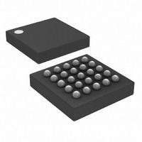
DS1862B+ Maxim Integrated Products, DS1862B+ Datasheet - Page 20

DS1862B+
Manufacturer Part Number
DS1862B+
Description
IC LASR CTRLR 7CHAN 5.5V 25CSBGA
Manufacturer
Maxim Integrated Products
Type
Laser Diode Controller (Fiber Optic)r
Datasheet
1.DS1862B.pdf
(43 pages)
Specifications of DS1862B+
Data Rate
10Gbps
Number Of Channels
7
Voltage - Supply
2.9 V ~ 5.5 V
Current - Supply
3mA
Operating Temperature
-40°C ~ 100°C
Package / Case
25-CSBGA
Mounting Type
Surface Mount
Lead Free Status / RoHS Status
Lead free / RoHS Compliant
XFP Laser Control and Digital Diagnostic IC
/* Assume that the Null input is 0.5V. */
/* In addition, the requirement for LSB is 50μV. */
/* Thus the NULL input of 0.5V and the 90% of FS input
is 2.94912V. */
The gain register is now set and the resolution of the
conversion will best match the expected LSB. The next
step is to calibrate the offset of the DS1862. With the
correct gain value written to the gain register, again
force the NULL input to the monitor pin. Read the digi-
tal result from the part (Meas1). The offset value is
equal to negative value of Meas1.
The calculated offset is now written to the DS1862 and
the gain and offset-scaling procedure is complete.
20
FS = 65536 * 50e-6;
CNT1 = 0.5 / 50e-6;
CNT2 = 0.90*FS / 50e-6;
set the trim-offset-register to zero;
set Right-Shift register to zero (Typically zero.
See the Right-Shifting section);
gain_result = 0h;
CLAMP = FFF8h/2^(Right_Shift_Register);
For n = 15 down to 0
begin
If Meas2 >= CLAMP then
Else
end;
Set the gain register to gain_result;
____________________________________________________________________
gain_result = gain_result + 2^n;
Force the 90% FS input (2.94912V);
Meas2 = read the digital result from the part;
gain_result = gain_result - 2^n;
Force the NULL input (0.5V);
Meas1 = read the digital result from the part;
if (Meas2 - Meas1) > (CNT2 - CNT1) then
gain_result = gain_result - 2^n;
OFFSET REGISTER
_
=
⎡
⎢
⎣
/* 3.2768 */
/* 10000 */
/* 58982 */
( )
−
1
Meas
4
1
⎤
⎥
⎦
Table 10. Right-Shifting Selection
Right-shifting is a digital method used to regain some
of the lost ADC range of a calibrated system. If right-
shifting is enabled, by simply loading a non-zero value
into the appropriate Right-Shifting Register, then the
DS1862 shifts the calibrated result just before it is
stored into the monitor channels’ register. If a system is
calibrated so the maximum expected input results in a
digital output value of less than 7FFFh (50% of FS),
then it is a candidate for using the right-shifting
method.
If the maximum desired digital output is less than
7FFFh, then the calibrated system is using less than 1/2
the ADC’s range. Similarly, if the maximum desired dig-
ital output is less than 1FFFh, then the calibrated sys-
tem is only using 1/8th the ADC’s range. For example, if
an applied maximum analog signal yields a maximum
digital output less than 1FFCh, then only 1/8th of the
ADC’s range is used. Right-shifting improves the reso-
lution of the measured signal as part of internal calibra-
tion. Without right-shifting, the 3 MS bits of the ADC will
never be used. In this example, a value of 3 for the
right-shifting maximizes the ADC range and a larger
gain setting must be loaded to achieve optimal conver-
sion. No resolution is lost since this is a 13-bit converter
that is left justified. The value can be right-shifted 3
times without losing any resolution. The following table
describes when the right-shifting method can be effec-
tively used.
OUTPUT RANGE USED WITH
ZERO RIGHT-SHIFTS
Right-Shifting A/D Conversion Result
0h .. FFFFh
0h .. 7FFFh
0h .. 3FFFh
0h .. 1FFFh
0h .. 0FFFh
(Scalable Dynamic Ranging)
NUMBER OF RIGHT-
SHIFTS NEEDED
0
1
2
3
4


