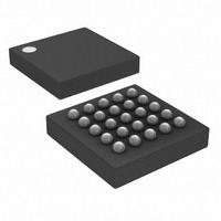
DS1862B+ Maxim Integrated Products, DS1862B+ Datasheet - Page 36

DS1862B+
Manufacturer Part Number
DS1862B+
Description
IC LASR CTRLR 7CHAN 5.5V 25CSBGA
Manufacturer
Maxim Integrated Products
Type
Laser Diode Controller (Fiber Optic)r
Datasheet
1.DS1862B.pdf
(43 pages)
Specifications of DS1862B+
Data Rate
10Gbps
Number Of Channels
7
Voltage - Supply
2.9 V ~ 5.5 V
Current - Supply
3mA
Operating Temperature
-40°C ~ 100°C
Package / Case
25-CSBGA
Mounting Type
Surface Mount
Lead Free Status / RoHS Status
Lead free / RoHS Compliant
XFP Laser Control and Digital Diagnostic IC
The DS1862 features two separate and independent
32-bit passwords for important memory locations. The
host password and the module password allow their
own allocated memory locations to be locked to pre-
vent write and/or read access. To enhance the security
of the DS1862, the password entry and setting bytes
can never be read.
To gain access to host-protected or module-protected
memory locations, the correct 32-bit value must be
entered into the password entry bytes (PWE) in either a
single 4-byte write, or 4 single-byte writes. To reprogram
either password, simply enter the appropriate current
password to gain memory access, write the new Host or
module PW with one 4-byte write, and finally re-enter the
new password into the PWE to regain memory access.
The DS1862 does require a particular power-up
sequence to ensure proper functionality. V
always be applied first or at the same time as V
this power-up sequence is not followed, then current can
be sourced out of V
with a resistor internal to the DS1862. If V
then it should be externally connected to V
The EN1 and EN2 output pins are controlled by the bits
at address 01h, bits 2 and 1. The logic state of the pins
is directly analogous to the logical state of the register.
EN1 and EN2 automatically change to a high and low
state, respectively, during power-down mode as
described in the Power-Down Functionality section.
A programmable voltage source, THRSET, is also pro-
vided for use with signal conditioners. This source is
programmable from 0 to 1V in 256 increments.
The DS1862 supports I
transfers with PEC. The slave address is unalterable
and is set to A0h. The DS1862, however, does have an
additional dedicated pin, MOD-DESEL, which acts as
an active-low chip select to enable communication. See
the I
Packet Error Checking sections for details.
36
2
____________________________________________________________________
C Serial Interface and the I
Security/Password Protection
Signal Conditioners—EN1 and EN2
Checking (PEC) Information
CC2
EN1 and EN2 and THRSET
Signal Conditioners—THRSET
2
C data transfers as well as data
as if it was connected to V
Signal Conditioners—
I
Power-Up Sequence
2
C and Packet Error
2
C Operation Using
CC2
CC3
CC3
is not used
.
should
CC2
CC3
. If
The DS1862 features a factory-trimmed SCALE value
for use with DS60 or LM50 temperature sensors. If
external temperature measurement on AUX2MON is
used with one of these two sensors, the 16-bit SCALE
value can be read from Table 05h and written into the
SCALE register in Table 04h, Byte 9Ch and 9Dh. This
option allows for the most precise setting for SCALE
without requiring additional trimming. Since the SCALE
register value is precisely trimmed at the factory, the
OFFSET register will always be a nonunique value and
can simply be written into the OFFSET register. For the
DS60, the value of EF0Ah in OFFSET completes the
internal calibration. For the LM50, the value of F380h in
OFFSET completes the internal calibration.
The following terminology is commonly used to describe
I
Master device: The master device controls the slave
devices on the bus. The master device generates SCL
clock pulses and START and STOP conditions.
Slave devices: Slave devices send and receive data at
the master’s request.
Bus idle or not busy: Time between STOP and START
conditions when both SDA and SCL are inactive and in
their logic-high states.
START condition: A START condition is generated by
the master to initiate a new data transfer with a slave.
Transitioning SDA from high to low while SCL remains
high generates a START condition. See Figure 14 for
applicable timing.
STOP condition: A STOP condition is generated by the
master to end a data transfer with a slave. Transitioning
SDA from low to high while SCL remains high generates
a STOP condition. See Figure 14 for applicable timing.
REPEATED START condition: The master can use a
REPEATED START condition at the end of one data
transfer to indicate that it will immediately initiate a new
data transfer following the current one. REPEATED
STARTs are commonly used during read operations to
identify a specific memory address to begin a data trans-
fer. A REPEATED START condition is issued identically
to a normal START condition. See Figure 14 for applica-
ble timing.
2
C data transfers.
Precision SCALE Register
I
2
Settings for AUX2MON
C Serial Interface
I
2
C Definitions


