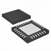
MAX16812ATI+ Maxim Integrated Products, MAX16812ATI+ Datasheet - Page 11

MAX16812ATI+
Manufacturer Part Number
MAX16812ATI+
Description
IC LED DRIVR HIGH BRIGHT 28-TQFN
Manufacturer
Maxim Integrated Products
Type
HBLED Driverr
Datasheet
1.MAX16812ATI.pdf
(21 pages)
Specifications of MAX16812ATI+
Constant Current
Yes
Topology
PWM, SEPIC, Step-Down (Buck), Step-Up (Boost)
Number Of Outputs
1
Internal Driver
Yes
Type - Primary
Automotive
Type - Secondary
High Brightness LED (HBLED)
Frequency
125kHz ~ 500kHz
Voltage - Supply
5.5 V ~ 76 V
Mounting Type
Surface Mount
Package / Case
28-TQFN Exposed Pad
Operating Temperature
-40°C ~ 125°C
Internal Switch(s)
Yes
Number Of Segments
2
Low Level Output Current
1.2 mA
High Level Output Current
1 A
Operating Supply Voltage
5.5 V to 76 V
Maximum Supply Current
2.5 mA
Maximum Power Dissipation
2759 mW
Maximum Operating Temperature
+ 125 C
Mounting Style
SMD/SMT
Minimum Operating Temperature
- 40 C
Lead Free Status / RoHS Status
Lead free / RoHS Compliant
Voltage - Output
-
Current - Output / Channel
-
Efficiency
-
Lead Free Status / Rohs Status
Lead free / RoHS Compliant
A high-side transconductance amplifier converts the
voltage across the LED current-sense resistor (R
into an internal current output. This current flows
through an internal resistor connected to AGND. The
voltage gain for the LED current-sense signal is 4. The
amplified signal is then buffered and connected
through an internal switch to CS_OUT.
The MAX16812 includes a built-in voltage-error amplifi-
er, which can be used to close the feedback loop. The
internal LED current-sense output signal is buffered
internally and then connected to CS_OUT through an
internal switch. CS_OUT is connected to the inverting
input (FB) pin of the error amplifier through a resistor.
See Figures 4 and 5. The reference voltage for the out-
put current is connected to REFI, the noninverting input
of the error amplifier. When the internal dimming signal
Figure 4. Internal Error Amplifier Connection (Dimming Signal High)
Figure 5. Internal Error Amplifier Connections (Dimming Signal Low)
High-Side Current-Sense Output (CS_OUT)
______________________________________________________________________________________
with Analog and PWM Dimming Control
Internal Error Amplifier
X1
X1
Integrated High-Voltage LED Driver
STATE B
STATE A
OUT
OUT
R
CS
R
COMP1
COMP1
REFI
)
REFI
is low, COMP is disconnected from the output of the
error amplifier and CS_OUT is simultaneously discon-
nected from the buffered LED current-sense output sig-
nal (Figure 5). When the internal dimming signal is high,
the output of the op amp is connected to COMP and
CS_OUT is connected to the buffered LED current-
sense signal at the same time (Figure 4). This enables
the compensation capacitor to hold the charge when
the DIM signal has turned off the internal switching
MOSFET gate drive. To maintain the charge on the
compensation capacitors C
capacitors should be of the low-leakage ceramic type.
When the internal dimming signal is enabled, the voltage
on the compensation capacitor forces the converter into
steady state almost instantaneously. The voltage on
COMP is subtracted from the internal slope compensa-
tion signal and is then connected to one of the inputs of
the PWM comparator. The PWM comparator input is of
the CMOS type with very low bias currents.
R
R
COMP2
COMP2
EA
EA
C
C
COMP2
COMP2
C
C
COMP1
COMP1
COMP1
COMP
COMP
and C
COMP2
, the
11


