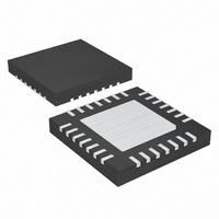
MAX16812ATI+ Maxim Integrated Products, MAX16812ATI+ Datasheet - Page 7

MAX16812ATI+
Manufacturer Part Number
MAX16812ATI+
Description
IC LED DRIVR HIGH BRIGHT 28-TQFN
Manufacturer
Maxim Integrated Products
Type
HBLED Driverr
Datasheet
1.MAX16812ATI.pdf
(21 pages)
Specifications of MAX16812ATI+
Constant Current
Yes
Topology
PWM, SEPIC, Step-Down (Buck), Step-Up (Boost)
Number Of Outputs
1
Internal Driver
Yes
Type - Primary
Automotive
Type - Secondary
High Brightness LED (HBLED)
Frequency
125kHz ~ 500kHz
Voltage - Supply
5.5 V ~ 76 V
Mounting Type
Surface Mount
Package / Case
28-TQFN Exposed Pad
Operating Temperature
-40°C ~ 125°C
Internal Switch(s)
Yes
Number Of Segments
2
Low Level Output Current
1.2 mA
High Level Output Current
1 A
Operating Supply Voltage
5.5 V to 76 V
Maximum Supply Current
2.5 mA
Maximum Power Dissipation
2759 mW
Maximum Operating Temperature
+ 125 C
Mounting Style
SMD/SMT
Minimum Operating Temperature
- 40 C
Lead Free Status / RoHS Status
Lead free / RoHS Compliant
Voltage - Output
-
Current - Output / Channel
-
Efficiency
-
Lead Free Status / Rohs Status
Lead free / RoHS Compliant
20, 21
22, 23
PIN
10
11
12
13
14
15
16
17
18
19
24
25
26
27
28
—
1
2
3
4
5
6
7
8
9
CS_OUT
H_REG
L_REG
NAME
COMP
AGND
SGND
TGRM
REFI
DGT
CS+
DRV
SRC
REF
DIM
CS-
SLP
DD
OV
EN
HV
GT
FB
LV
LX
RT
EP
IN
_______________________________________________________________________________________
with Analog and PWM Dimming Control
Low-Side Error Amplifier’s Inverting Input
Low-Side Error Amplifier’s Output. Connect a compensation network from COMP to FB for stable operation.
Reference Input. V
LED current.
+1.23V Reference Output. Connect an appropriate soft-start capacitor from REF to AGND.
High-Side Current-Sense Amplifier Output. V
Analog Ground
Enable Input/Undervoltage Lockout. Connect EN to IN through a resistive voltage-divider to program the
UVLO threshold. Connect EN directly to IN to set up the device for 5V internal threshold. Apply a logic-
level input to EN to enable/disable the device.
Positive Power-Supply Input. Bypass with a 1µF ceramic capacitor to AGND.
5V Low-Side Regulator Output. Bypass with a 3.3µF ceramic capacitor to AGND.
Signal Ground
MOSFET’s Drain Voltage-Sense Input. Connect DD to the drain of the external dimming MOSFET.
External Dimming MOSFET’s Gate Drive
High-Side Current-Sense Amplifier’s Positive Input. Connect R
referenced to LV.
High-Side Current-Sense Amplifier’s Negative Input. Connect R
referenced to LV.
High-Side Reference Voltage Input. A DC voltage at LV sets the lowest reference point for the high-side
current-sense and dimming MOSFET control circuitry.
High-Side Regulator Output. H_REG provides a regulated supply for high-side circuitry. Bypass with a 1µF
ceramic capacitor to LV.
High-Side Positive Supply Voltage Input. HV provides power for dimming and LED current-sense circuitry.
HV is referenced to LV.
Internal MOSFET Gate Driver Output. Connect to a resistor between DRV and GT to set the rise and fall
times at LX.
Internal MOSFET GATE. Connect a resistor between GT and DRV to set the rise and fall times at LX.
Internal MOSFET Drain
Internal Power MOSFET Source
Slope Compensation Setting. Connect an appropriate external capacitor from SLP to AGND to generate a
ramp signal for stable operation.
Dimming Comparator’s Reference/Ramp Generator
Dimming Control Input
Resistor-Programmable Internal Oscillator Setting. Connect a resistor from RT to AGND to set the internal
oscillator frequency.
Overvoltage Protection Input. Connect OV to HI through a resistive voltage-divider to AGND to set the
overvoltage limit for the load. When the voltage at OV exceeds the 1.238V (typ) threshold, the gate drive
(DRV) for the switching MOSFET is disabled. Once V
MOSFET turns on again.
Exposed Pad. Connect EP to a large-area ground plane for effective power dissipation. Do not use as the
IC ground connection.
Integrated High-Voltage LED Driver
REFI
provides the reference voltage for the high-side current-sense amplifier to set the
CS_OUT
FUNCTION
is proportional to the current through R
OV
goes below 1.238V by 14mV, the switching
CS
CS
between CS+ and CS-. CS+ is
between CS- and CS+. CS- is
Pin Description
CS
.
7


