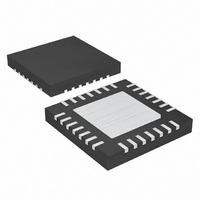
MAX16812ATI+ Maxim Integrated Products, MAX16812ATI+ Datasheet - Page 2

MAX16812ATI+
Manufacturer Part Number
MAX16812ATI+
Description
IC LED DRIVR HIGH BRIGHT 28-TQFN
Manufacturer
Maxim Integrated Products
Type
HBLED Driverr
Datasheet
1.MAX16812ATI.pdf
(21 pages)
Specifications of MAX16812ATI+
Constant Current
Yes
Topology
PWM, SEPIC, Step-Down (Buck), Step-Up (Boost)
Number Of Outputs
1
Internal Driver
Yes
Type - Primary
Automotive
Type - Secondary
High Brightness LED (HBLED)
Frequency
125kHz ~ 500kHz
Voltage - Supply
5.5 V ~ 76 V
Mounting Type
Surface Mount
Package / Case
28-TQFN Exposed Pad
Operating Temperature
-40°C ~ 125°C
Internal Switch(s)
Yes
Number Of Segments
2
Low Level Output Current
1.2 mA
High Level Output Current
1 A
Operating Supply Voltage
5.5 V to 76 V
Maximum Supply Current
2.5 mA
Maximum Power Dissipation
2759 mW
Maximum Operating Temperature
+ 125 C
Mounting Style
SMD/SMT
Minimum Operating Temperature
- 40 C
Lead Free Status / RoHS Status
Lead free / RoHS Compliant
Voltage - Output
-
Current - Output / Channel
-
Efficiency
-
Lead Free Status / Rohs Status
Lead free / RoHS Compliant
ABSOLUTE MAXIMUM RATINGS
(All voltages are referenced to AGND, unless otherwise noted.)
SGND ....................................................................-0.3V to +0.3V
IN, EN, LX, DIM ......................................................-0.3V to +80V
L_REG, GT, DRV ......................................................-0.3V to +6V
RT, REF, REFI, CS_OUT, FB, COMP, SRC,
LV, HV, CS-, CS+, DGT, DD, H_REG ....................-0.3V to +80V
CS+, DGT, H_REG to LV ........................................-0.3V to +12V
CS- to LV ...............................................................-0.3V to +0.3V
CS+ to CS- .............................................................-0.3V to +12V
Integrated High-Voltage LED Driver
with Analog and PWM Dimming Control
*As per JEDEC51 standard (multilayer board).
Stresses beyond those listed under “Absolute Maximum Ratings” may cause permanent damage to the device. These are stress ratings only, and functional
operation of the device at these or any other conditions beyond those indicated in the operational sections of the specifications is not implied. Exposure to
absolute maximum rating conditions for extended periods may affect device reliability.
ELECTRICAL CHARACTERISTICS
(V
erwise noted. Typical values are at T
2
Input Voltage Range
Quiescent Supply
Shutdown Supply Current
Internal MOSFET On-Resistance
Output Current Accuracy
Peak Switch Current Limit
Hiccup Switch Current
Switch Leakage Current
UNDERVOLTAGE LOCKOUT
IN Undervoltage Lockout
UVLO Hysteresis
EN Threshold Voltage
EN Hysteresis
REFERENCE (REF) AND LOW-SIDE LINEAR REGULATOR (L_REG)
Startup Response Time
Reference Voltage
Reference Soft-Start Charging
Current
L_REG Supply Voltage
L_REG Load Regulation
L_REG Dropout Voltage
IN
SLP, TGRM, OV ....................................................-0.3V to +6V
_______________________________________________________________________________________
= V
EN
PARAMETER
= 12V, C
L_REG
= 3.3µF, C
I
V
A
SYMBOL
REF_SLEW
I
H_REG
R
EN_THUP
LXLEAK
I
I
= +25°C.)
UVLO
SHDN
LXLIM
V
t
I
DSON
V
POR
LED
REF
I
Q
IN
= 1µF, C
V
V
I
I
V
V
V
V
I
V
V
I
I
LX
LED
REF
L_REG
L_REG
TGRM
EN
EN
IN
EN
IN
REF
IN
= 1A, V
rising
or V
= 7.5V, I
REF
≤ 300mV
= 0V, V
rising
= 350mA, R
= 10µA
= 0V
= 20mA
= 25mA
= 1V, V
EN
= 47nF, V
IN
rising
LX
L_REG
> 10V, V
DIM
= 76V, V
CONDITIONS
CS
TGRM
= 0V
= 1mA
= 1Ω
DD to LV ....................................................................-1V to +80V
Maximum Current into Any Pin (except LX, SRC) ............±20mA
Maximum Current into LX and SRC.......................................+2A
Continuous Power Dissipation (T
Operating Temperature Range .........................-40°C to +125°C
Junction Temperature ......................................................+150°C
Storage Temperature Range .............................-65°C to +150°C
Lead Temperature (soldering, 10s) .................................+300°C
GT
28-Pin TQFN 5mm x 5mm
(derate 34.65mW/°C* above +70°C) .........................2759mW
GT
= 0V, R
= V
= 0V
DRV
SRC
= 5V
= 0.2Ω, T
A
1.190
= T
MIN
5.5
0.3
2.6
4.6
1.2
4.9
25
-5
J
A
= -40°C to +125°C, unless oth-
= +70°C)
1.238
TYP
1.38
100
100
400
0.2
3.1
4.9
5.2
20
50
40
6
1
1.288
MAX
76.0
2.5
0.4
3.6
5.3
1.6
5.5
45
+5
10
60
20
UNITS
mA
mV
mV
mV
µA
µA
µA
µs
%
Ω
A
A
Ω
V
V
V
V
V


