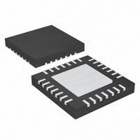
MAX16812ATI+ Maxim Integrated Products, MAX16812ATI+ Datasheet - Page 9

MAX16812ATI+
Manufacturer Part Number
MAX16812ATI+
Description
IC LED DRIVR HIGH BRIGHT 28-TQFN
Manufacturer
Maxim Integrated Products
Type
HBLED Driverr
Datasheet
1.MAX16812ATI.pdf
(21 pages)
Specifications of MAX16812ATI+
Constant Current
Yes
Topology
PWM, SEPIC, Step-Down (Buck), Step-Up (Boost)
Number Of Outputs
1
Internal Driver
Yes
Type - Primary
Automotive
Type - Secondary
High Brightness LED (HBLED)
Frequency
125kHz ~ 500kHz
Voltage - Supply
5.5 V ~ 76 V
Mounting Type
Surface Mount
Package / Case
28-TQFN Exposed Pad
Operating Temperature
-40°C ~ 125°C
Internal Switch(s)
Yes
Number Of Segments
2
Low Level Output Current
1.2 mA
High Level Output Current
1 A
Operating Supply Voltage
5.5 V to 76 V
Maximum Supply Current
2.5 mA
Maximum Power Dissipation
2759 mW
Maximum Operating Temperature
+ 125 C
Mounting Style
SMD/SMT
Minimum Operating Temperature
- 40 C
Lead Free Status / RoHS Status
Lead free / RoHS Compliant
Voltage - Output
-
Current - Output / Channel
-
Efficiency
-
Lead Free Status / Rohs Status
Lead free / RoHS Compliant
The MAX16812 is a current-mode PWM LED driver
with an integrated 0.2Ω power MOSFET for use in dri-
ving HB LEDs. By using two current regulation loops,
5% LED current accuracy is achieved. One current reg-
ulation loop controls the internal MOSFET peak current
through a sense resistor (R
while the other current regulation loop controls the
average LED current in a single LED string through
another sense resistor (R
The MAX16812 includes a cycle-by-cycle current limit
that turns off the gate drive to the internal MOSFET dur-
ing an overcurrent condition. The MAX16812 features a
programmable oscillator that simplifies and optimizes
the design of magnetics. The MAX16812 is well suited
for inputs from 5.5V to 76V. An external resistor in
series with the internal MOSFET gate can control the
rise and fall times on the drain of the internal switching
MOSFET, therefore minimizing EMI problems.
The MAX16812 high-frequency, current-mode PWM
HB LED driver integrates all the necessary building
blocks for driving a series LED string in an adjustable
constant current mode with PWM dimming. Current-
mode control with leading-edge blanking simplifies
control-loop design, and an external adjustable slope-
compensation control stabilizes the inner current-mode
loop when operating at duty cycles above 50%.
An input undervoltage lockout (UVLO) programs the
input supply startup voltage. An external voltage-
divider on EN programs the supply startup voltage. If
EN is directly connected to the input, the UVLO is set at
5V. A single external resistor from RT to AGND pro-
grams the switching frequency from 125kHz to 500kHz.
Wide contrast (100:1) PWM dimming can be achieved
with the MAX16812. A DC input on DIM controls the
dimming duty cycle. The dimming frequency is set by
the sawtooth ramp frequency on TGRM (see the PWM
Dimming section). In addition, PWM dimming can be
achieved by applying a PWM signal to DIM with TGRM
set to a DC voltage less than 1.238V. A floating high-
voltage driver drives an external n-channel MOSFET in
series with the LED string. REFI allows analog dimming
of the LED current, further increasing the effective dim-
ming range over PWM alone. The MAX16812 has a 5µs
preprogrammed LED current rise and fall time.
A nonlatching overvoltage protection limits the voltage
on the internal switching MOSFET under open-circuit
conditions in the LED string. The internal thermal shut-
down circuit protects the device if the junction tempera-
ture should exceed +165°C.
_______________________________________________________________________________________
with Analog and PWM Dimming Control
Detailed Description
CS
) in series with the LEDs.
SRC
Integrated High-Voltage LED Driver
) from SRC to ground,
The MAX16812 offers a current-mode control operation
feature with leading-edge blanking that blanks the
sensed current signal applied to the input of the PWM
current-mode comparator. In addition, a current-limit
comparator monitors the same signal at all times and
provides cycle-by-cycle current limit. An additional hic-
cup comparator limits the absolute peak current to two
times the cycle-by-cycle current limit. The leading-edge
blanking of the current-sense signal prevents noise at
the PWM comparator input from prematurely terminat-
ing the on-cycle. The switch current-sense signal con-
tains a leading-edge spike that results from the
MOSFET gate-charge current, and the capacitive and
diode reverse-recovery current of the power circuit. The
MAX16812’s capacitor-adjustable slope-compensation
feature allows for easy stabilization of the inner switch-
ing MOSFET current-mode loop. Upon triggering the
hiccup current limit, the soft-start capacitor on REF is
discharged and the gate drive to DRV is disabled.
Once the inductor current falls below the hiccup cur-
rent limit, the soft-start capacitor is released and it
begins to charge after 10µs.
The MAX16812 uses an internal ramp generator for
slope compensation. The internal ramp signal resets at
the beginning of each cycle and slews at the rate pro-
grammed by the external capacitor connected at SLP
and an internal I
nal attenuator attenuates the actual slope compensa-
tion signal by a factor of 0.2. Adjust the MAX16812
slew-rate capacitor by using the following equation:
where I
the slope compensation capacitance on the SLP in µF,
and SR is the designed slope in mV/µs.
When using the MAX16812 for internal switching MOS-
FET duty cycles greater than 50%, the following condi-
tions must be met to avoid current-loop subharmonic
oscillations.
where R
µH. L is the inductor connected to the LX pin of the
internal switching MOSFET and V
across the inductor during the off-time of the internal
MOSFET.
SLP
SR
SRC
is the charging current in mA and C
≥
is in mΩ, V
0 5
.
C
SLP
SLOPE
×
R
current source of 150µA. An inter-
SRC
IND_OFF
=
L
×
Current-Mode Control
0 2
Slope Compensation
.
V
IND OFF
×
is in volts, and L is in
IND_OFF
I
_
SLP
SR
mV
is the voltage
/
µ
s
SLOPE
is
9


