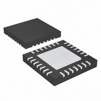
MAX16812ATI+ Maxim Integrated Products, MAX16812ATI+ Datasheet - Page 18

MAX16812ATI+
Manufacturer Part Number
MAX16812ATI+
Description
IC LED DRIVR HIGH BRIGHT 28-TQFN
Manufacturer
Maxim Integrated Products
Type
HBLED Driverr
Datasheet
1.MAX16812ATI.pdf
(21 pages)
Specifications of MAX16812ATI+
Constant Current
Yes
Topology
PWM, SEPIC, Step-Down (Buck), Step-Up (Boost)
Number Of Outputs
1
Internal Driver
Yes
Type - Primary
Automotive
Type - Secondary
High Brightness LED (HBLED)
Frequency
125kHz ~ 500kHz
Voltage - Supply
5.5 V ~ 76 V
Mounting Type
Surface Mount
Package / Case
28-TQFN Exposed Pad
Operating Temperature
-40°C ~ 125°C
Internal Switch(s)
Yes
Number Of Segments
2
Low Level Output Current
1.2 mA
High Level Output Current
1 A
Operating Supply Voltage
5.5 V to 76 V
Maximum Supply Current
2.5 mA
Maximum Power Dissipation
2759 mW
Maximum Operating Temperature
+ 125 C
Mounting Style
SMD/SMT
Minimum Operating Temperature
- 40 C
Lead Free Status / RoHS Status
Lead free / RoHS Compliant
Voltage - Output
-
Current - Output / Channel
-
Efficiency
-
Lead Free Status / Rohs Status
Lead free / RoHS Compliant
Typically, there are two sources of noise emission in a
switching power supply: high di/dt loops and high dv/dt
surfaces. For example, traces that carry the drain cur-
rent often form high di/dt loops. Similarly, the drain of
the internal MOSFET connected to the LX pin presents
a dv/dt source. Keep all PCB traces carrying switching
currents as short as possible to minimize current loops.
Use ground planes for best results.
Careful PCB layout is critical to achieve low switching
losses and clean, stable operation. Use a multilayer
board whenever possible for better noise immunity and
power dissipation. Follow these guidelines for good
PCB layout:
Integrated High-Voltage LED Driver
with Analog and PWM Dimming Control
18
• Use a large copper plane under the MAX16812
• Isolate the power components and high-current
package. Ensure that all heat-dissipating compo-
nents have adequate cooling. Connect the exposed
pad of the device to the ground plane.
paths from sensitive analog circuitry.
______________________________________________________________________________________
Layout Recommendations
• Keep the high-current paths short, especially at the
• Connect AGND and SGND to a ground plane.
• Keep the power traces and load connections short.
• Ensure that the feedback connection to FB is short
• Route high-speed switching nodes away from the
• To prevent discharge of the compensation capaci-
ground terminals. This practice is essential for stable,
jitter-free operation. Keep switching loops short.
Ensure a low-impedance connection between all
ground points.
This practice is essential for high efficiency. Use
thick copper PCBs to enhance full-load efficiency.
and direct.
sensitive analog areas.
tors, C
the dimming cycle, ensure that the PCB area close
to these components has extremely low leakage.
COMP1
and C
COMP2
, during the off-time of


