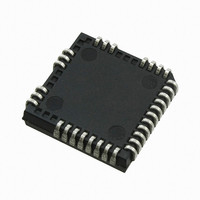
IRS26310DJPBF International Rectifier, IRS26310DJPBF Datasheet - Page 33

IRS26310DJPBF
Manufacturer Part Number
IRS26310DJPBF
Description
IC DRIVER BRIDGE 3-PHASE 44-PLCC
Manufacturer
International Rectifier
Datasheet
1.IRS26310DJTRPBF.pdf
(41 pages)
Specifications of IRS26310DJPBF
Configuration
3 Phase Bridge
Input Type
Non-Inverting
Delay Time
530ns
Current - Peak
200mA
Number Of Configurations
1
Number Of Outputs
3
High Side Voltage - Max (bootstrap)
600V
Voltage - Supply
12 V ~ 20 V
Operating Temperature
-40°C ~ 125°C
Mounting Type
Surface Mount
Package / Case
44-PLCC (32 Leads)
Peak Output Current
200mA
Input Delay
530ns
Output Delay
530ns
Supply Voltage Range
12V To 20V
Driver Case Style
LCC
No. Of Pins
44
Operating Temperature Range
-40°C To +125°C
Rohs Compliant
Yes
Device Type
High Side / Low Side
Family Hvic
General Purpose HVICs
Channels
6
Topology
Three Phase
Application
General Purpose / Motor Control / PDP
Voffset
600
Io+ (ma)
200
Io- (ma)
350
Shutdown / Reset
Yes
Separate Power And Logic Ground
Yes
Integrated Bootstrap Diode
Yes
Over Current Protection
Yes
Uvlo
Vcc / Vbs
Vbsuv+ / Vccuv+ Min (v)
10.4
Vbsuv+ / Vccuv+ Typ (v)
11.1
Vbsuv+ / Vccuv+ Max (v)
11.6
Vbsuv- / Vccuv- Min (v)
10.2
Vbsuv- / Vccuv- Typ (v)
10.9
Dt / Sdt Min (ns)
190
Dt / Sdt Typ (ns)
290
Dt / Sdt Max (ns)
420
T On Min (ns)
400
T On Typ (ns)
530
T On Max (ns)
750
T Off Min (ns)
400
T Off Typ (ns)
530
T Off Max (ns)
750
Fault Reporting
Yes
Package
44 Lead
Part Status
Active & Preferred
Special Features
DC Bus Sensing with Over Voltage Protection
Lead Free Status / RoHS Status
Lead free / RoHS Compliant
Available stocks
Company
Part Number
Manufacturer
Quantity
Price
Company:
Part Number:
IRS26310DJPBF
Manufacturer:
International Rectifier
Quantity:
10 000
Supply Capacitor: It is recommended to place a bypass capacitor (C
connection is shown in Figure 35. A ceramic 1 μF ceramic capacitor is suitable for most applications. This
component should be placed as close as possible to the pins in order to reduce parasitic elements.
Routing and Placement: Power stage PCB parasitic elements can contribute to large negative voltage transients at
the switch node; it is recommended to limit the phase voltage negative transients. In order to avoid such conditions,
it is recommended to 1) minimize the high-side emitter to low-side collector distance, and 2) minimize the low-side
emitter to negative bus rail stray inductance. However, where negative V
may be taken to reduce the spike. This includes placing a resistor (5 Ω or less) between the V
node (see Figure 36), and in some cases using a clamping diode between V
at
Additional Documentation
Several technical documents related to the use of HVICs are available at www.irf.com; use the Site Search
function and the document number to quickly locate them. Below is a short list of some of these documents.
DT97-3: Managing Transients in Control IC Driven Power Stages
AN-1123: Bootstrap Network Analysis: Focusing on the Integrated Bootstrap Functionality
DT04-4: Using Monolithic High Voltage Gate Drivers
AN-978: HV Floating MOS-Gate Driver ICs
www.irf.com
www.irf.com
for more detailed information.
Figure 36: V
S
resistor
C
IN
Figure 35: Supply capacitor
HIN (x3)
LIN (x3)
FAULT
ITRIP
RCIN
EN
V
V
SS
cc
33
Figure 37: V
LO (x3)
COM
V
B
(x3)
IN
V
HO (x3)
) between the V
S
S
(x3)
SS
spikes remain excessive, further steps
and V
S
IRS26310DJPbF
clamping diode
S
(see Figure 37). See DT04-4
© 2008 International Rectifier
CC
and V
S
pin and the switch
SS
pins. This


