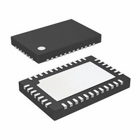
ISL97522IRZ-T Intersil, ISL97522IRZ-T Datasheet

ISL97522IRZ-T
Specifications of ISL97522IRZ-T
Related parts for ISL97522IRZ-T
ISL97522IRZ-T Summary of contents
Page 1
... A external transistor is required). Ordering Information PART NUMBER PART TAPE & (Note) MARKING REEL ISL97522IRZ-TK ISL 97522IRZ 13” (1k pcs) ISL97522IRZ-T ISL 97522IRZ 13” (4k pcs) NOTE: Intersil Pb-free plus anneal products employ special Pb-free material sets; molding compounds/die attach materials and 100% matte tin plate termination finish, which are RoHS compliant and compatible with both SnPb and Pb-free soldering operations ...
Page 2
Absolute Maximum Ratings (T A Maximum Pin Voltages, all pins except below . . . . . . . . . . . . . . 6.5V VIN,EN,ENL,LX,VHIL ...
Page 3
Electrical Specifications PARAMETER DESCRIPTION I Peak Drive Current PEAKB I I Output Current ISADJB SADJB I I Output Current ILADJB LADJB V LDO ON V FBP Regulation Voltage FBP V FBP Fault Trip Point F_FBP ...
Page 4
Electrical Specifications PARAMETER DESCRIPTION t fall CTL to OUT Falling Prop Delay D V SRC Input Voltage Range SRC ISRC SRC Input Current R SRC SRC On Resistance ON R DRN DRN On Resistance ON ...
Page 5
Typical Performance Curves 100 5V 12V IN VDD 12V 17V IN VDD 500 1000 1500 I (mA) AVDD FIGURE 1. BOOST ...
Page 6
Typical Performance Curves -8.875 -8.880 V = -9V OFF -8.885 -8.890 -8.895 -8.900 -8.905 (mA) VOFF FIGURE 7. V LOAD REGULATION OFF CDLY EN A VDD V LOGIC FIGURE 9. START-UP SEQUENCE A VDD I IN ...
Page 7
Typical Performance Curves A VDD I IN FIGURE 13. IN RUSH CURRENT 7 ISL97522 (Continued) (BUCK) V (BUCK MODE) LOGIC I IN FIGURE 14. IN RUSH CURRENT December 13, 2006 FN7445.0 ...
Page 8
Pin Descriptions PIN # PIN NAME 1 DRVN Negative LDO base drive; open drain of an internal P-Channel MOSFET. 2 DELB Active low control output for optional delay control for external A goes to high. 3 FBW Negative LDO voltage ...
Page 9
Typical Application Diagram V IN 10µFX2 V IN C30 R10 10kΩ C1 4.7NF CINTB I R20 30k SADJB R19 30k I LADJB V DCP C23 INTERNAL 4.7µF V SUPPLY DC C24 4.7µF POWER ON CDLY SEQUENCING C7 220nF EN R29 ...
Page 10
Applications Information The ISL97522 provides a multiple output power supply solution for TFT-LCD applications. The system consists of a high efficiency boost controller, two low cost linear-regulator controllers (V and V ) and a buck reglator (V ON OFF Table ...
Page 11
V REF REFERENCE GENERATOR FBB GM AMPLIFIER CINTB UVLO COMPARATOR FIGURE 15. FUNCTION DIAGRAM OF THE BOOST CONTROLLER The internal current limit circuitry is shown in Figure 16. The circuit senses the voltage across the R MOSFET is on; then ...
Page 12
D is the duty cycle – ----------------------- - = overcome the variation in external LX driver R input is provided (ILADJ) to accommodate 5 different bands ...
Page 13
PI mode and R (R INT 23 INT The IC is designed to operate with a minimum C of 4.7nF and a minimum C (effective) = 10µF. 2 Note that, for high voltage A , the voltage ...
Page 14
LDO_OFF PG_LDON - + R 0.4V FBN DRVN + GMN R BN 36V 3kΩ ESD CLAMP FIGURE 18. V FUNCTION BLOCK DIAGRAM OFF The V power supply is used to power the positive supply ON ...
Page 15
CHARGE PUMP V IN OUTPUT OR A VDD 3kΩ DRVP NPN CASCODE TRANSISTOR ISL97522 FBP FIGURE 19. CASCODE NPN TRANSISTOR CONFIGURATION FOR HIGH CHARGE PUMP OUTPUT VOLTAGE (>36V) 0.1µF 0.1µF 3kΩ 0.1µF DRVP Q3 0.47µF 0.1µF ISL97522 FBP FIGURE 20. ...
Page 16
Buck Inductor An inductor value in the range 3.3-10µH is recommended for the buck converter. Besides the inductance, the DC resistance and the saturation current should also be considered when choosing buck inductor. Low DC resistance can help maintain high ...
Page 17
ISL97522 V CDLY EN ENL V LOGIC V REF V BOOST OFF t DEL1 DELAYED V BOOST SLICE ON START-UP SEQUENCE TIMED BY C FIGURE 21. ISL97522 START-UP SEQUENCE DEL2 ...
Page 18
Fault Protection During the startup sequence, prior to BOOST soft-start checked to be within ±20% of its final value and the REF device temperature is checked. If either of these are not within the expected range, the part ...
Page 19
The exposed die plate, on the underneath of the package, should be soldered to an equivalent area of metal on the PCB. This contact area should have multiple via connections to the back of the PCB as well as ...
Page 20
... Accordingly, the reader is cautioned to verify that data sheets are current before placing orders. Information furnished by Intersil is believed to be accurate and reliable. However, no responsibility is assumed by Intersil or its subsidiaries for its use; nor for any infringements of patents or other rights of third parties which may result from its use ...


