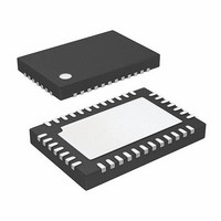
ISL97522IRZ-T Intersil, ISL97522IRZ-T Datasheet - Page 13

ISL97522IRZ-T
Manufacturer Part Number
ISL97522IRZ-T
Description
IC SUPPLY CTRL 4CH TFT-LCD 38QFN
Manufacturer
Intersil
Datasheet
1.ISL97522IRZ-T.pdf
(20 pages)
Specifications of ISL97522IRZ-T
Applications
LCD TV/Monitor
Current - Supply
3mA
Voltage - Supply
4.5 V ~ 13.2 V
Operating Temperature
-40°C ~ 85°C
Mounting Type
Surface Mount
Package / Case
38-QFN
Lead Free Status / RoHS Status
Lead free / RoHS Compliant
PI mode C
The IC is designed to operate with a minimum C
of 4.7nF and a minimum C
Note that, for high voltage A
ceramic capacitors (C
greatly; a 16V 10µF ceramic can drop to around 3µF at 15V.
To improve the transient load response of A
a resistor may be added in series with the C
larger the resistor the lower the overshoot but at the expense
of stability of the converter loop - especially at high currents.
With L = 10µH, A
should have a capacitance of greater than 10µF. R
can have values up to 5kΩ for C
up to 10K for C
Larger values of R
A
ensure A
maximum desired current and then the transient load
response of A
maximum value of R
Operation of the DELB Output Function
An open drain DELB output is provided to allow the boost
output voltage, developed at C
to be delayed via an external switch (Q3) to a time after the
V
have achieved regulation during the start-up sequence
shown in Figure 21. This then allows the A
supplies to start-up from 0V instead of the normal offset
voltage of V
When DELB is activated by the start-up sequencer, it sinks
50µA allowing a controlled turn-on of Q3 and charge-up of
C
reduce inrush current into C
by R
required by the voltage rating of this device. When the
voltage at DELB falls to less than 0.6V, the sink current is
increased to ~1.2mA to firmly pull DELB to 0V.
The voltage at DELB is monitored by the fault protection
circuit so that if the initial 50µA sink current fails to pull DELB
below ~0.6V after the start-up sequencing has completed,
then a fault condition will be detected and a fault time-out
ramp will be initiated on the C
Linear-Regulator Controllers (V
The ISL97522 includes two independent linear-regulator
controllers, in which one is a positive output voltage (V
and one is negative. The V
VDD
BOOST
9
. C
9
16
load currents less than the current limit are used. To
and R
can be used to control the turn-on time of Q3 to
VDD
supply and negative V
IN
INT
8
stability, the IC should be operated at the
VDD
-V
can be used to limit the V
2
DIODE
(C
(effective) up to 30µF.
VDD
INT
should be used to determine the
23
INT
) and R
2
= 15V, C
(R
) reduces their effective capacitance
(D
7
1
) may be possible if maximum
2
) if Q3 were not present.
ON
VDD
9
(effective) = 10µF.
13
. The potential divider formed
DEL
INT
23
2
and V
OFF
, the voltage coefficient of
2
(see application diagram),
= 4.7nF, C
(effective) up to 20µF and
capacitor (C
(R
charge pump supply
OFF
10
ON
GS
)
, V
linear-regulator
VDD
23
voltage of Q3 if
VDD
2
OFF
(effective)
capacitor. The
7
and V
).
23
in PI mode,
)
INT
capacitor
ON
(R
ON
7
),
)
ISL97522
controller function diagrams are shown in Figures 17,
and 18, respectively.
Calculation of the Linear Regulator Base-Emitter
Resistors ( R
For the pass transistor of the linear regulator, low frequency
gain (Hfe) and unity gain freq. (f
datasheet. The pass transistor adds a pole to the loop transfer
function at f
margin at low frequency, the best choice for a pass device is
often a high frequency low gain switching transistor. Further
improvement can be obtained by adding a base-emitter resistor
R
increase the pole frequency to: f
where re = KT/qIc. So choose the lowest value R
design as long as there is still enough base current (I
support the maximum output current (I
We will take as an example the V
Fairchild MMBT3906 PNP transistor is used as the external pass
transistor, Q11 in the application diagram, then for a maximum V
operating requirement of 50mA the data sheet indicates HFE_min =
30.
The base-emitter saturation voltage is: Vbe_max = 0.7V.
For the ISL97522, the minimum drive current is:
I_DRVP_min = 2mA.
The minimum base-emitter resistor, R
calculated as:
R
0.7V/(2mA - 50mA/30) = 2.1kΩ
This is the minimum value that can be used - so, we now
choose a convenient value greater than this minimum value;
say 3KΩ. Larger values may be used to reduce quiescent
current, however, regulation may be adversely affected, by
supply noise if R
0.9V
PG_LDOP
BE
BP
_min = V
(R
BP
FIGURE 17. V
, R
+
GMP
-
p
BL
= f
+
-
BE
, R
T
BP
_max/(I_DRVP_min - Ic/Hfe_min) =
/Hfe. Therefore, in order to maintain phase
BP
BN
1 : Np
and R
is made too high in value.
CLAMP
LDO_ON
in the Functional Block Diagram), which
ON
ESD
36V
FUNCTION BLOCK DIAGRAM
BN
DRVP
FBP
)
T
p
) are usually specified in the
= f
R
3kΩ
ON
BP
T
*(1+ Hfe *re/R
C
linear regulator. If a
BP
).
R
R
, can now be
P1
P2
A
VDD
CP (TO 36V)
V
December 13, 2006
BE
ON
0.1µF
BE
(TO 35V)
in the
B
0.1µF
C
) to
)/Hfe,
ON
ISINB
FN7445.0
ON


