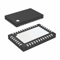
ISL97522IRZ-T Intersil, ISL97522IRZ-T Datasheet - Page 16

ISL97522IRZ-T
Manufacturer Part Number
ISL97522IRZ-T
Description
IC SUPPLY CTRL 4CH TFT-LCD 38QFN
Manufacturer
Intersil
Datasheet
1.ISL97522IRZ-T.pdf
(20 pages)
Specifications of ISL97522IRZ-T
Applications
LCD TV/Monitor
Current - Supply
3mA
Voltage - Supply
4.5 V ~ 13.2 V
Operating Temperature
-40°C ~ 85°C
Mounting Type
Surface Mount
Package / Case
38-QFN
Lead Free Status / RoHS Status
Lead free / RoHS Compliant
Buck Inductor
An inductor value in the range 3.3-10µH is recommended for
the buck converter. Besides the inductance, the DC
resistance and the saturation current should also be
considered when choosing buck inductor. Low DC
resistance can help maintain high efficiency, and the
saturation current rating should be at least maximum output
current plus half of ripple current.
Buck MOSFET
The principle to select Buck MOSFET is similar to that of
Boost. The voltage of stress of buck converter should be
maximum input voltage plus reasonable margin, and the
current rating should be over the maximum output current.
The r
20mΩ to 50mΩ.
Rectifier Diode (Buck Converter)
A Schottky diode is recommended due to fast recovery and
low forward voltage. The reverse voltage rating should be
higher than the maximum input voltage. The average current
should be as the following equation,
Where I
Output Capacitor (Buck Converter)
Four 10µF or two 22µF ceramic capacitors are
recommended for this part. The overshoot and undershoot
will be reduced with more capacitance, but the recovery time
will be longer.
PI Loop Compensation (Buck Converter)
The buck converter of ISL97522 can be compensated by a
RC network connected from CINTL pin to ground. C27 =
4.7nF and R17= 2k RC network is used in the demo board.
The larger value resistor can lower the transient overshoot,
however, at the expense of stability of the loop.
The stability can be optimized in a similar manner to that
described in the section on "PI Loop Compensation (Boost
Converter)”.
Bootstrap Capacitor (C28)
This capacitor is used to provide the supply to the high driver
circuitry for the buck MOSFET. The bootstrap supply is
formed by an internal diode and capacitor combination. A
1µF is recommended for ISL97522. A low value capacitor
can lead to overcharging and in turn damage the part.
If the load is too light, the on-time of the low side diode may
be insufficient to replenish the bootstrap capacitor voltage. In
this case, if V
device may be unable to turn-on until V
there is a minimum load requirement in this case. The
I
AVG
DS(ON)
=
(
O
1 D
is the output current of buck converter.
–
of this MOSFET should be in the range from
IN
)*I
-V
O
BUCK
< 1.5V, the internal MOSFET pull-up
16
LOGIC
falls. Hence,
(EQ. 19)
ISL97522
minimum load can be adjusted by the feedback resistors
to FBL.
The bootstrap capacitor can only be charged when the
higher side MOSFET is off. If the load is too light which can
not make the on time of the low side diode be sufficient to
replenish the boot strap capacitor, the MOSFET can’t turn
on. Hence there is minimum load requirement to charge the
bootstrap capacitor properly.
Start-Up Sequence
Figure 21 shows a detailed start-up sequence waveform. For
a successful power-up, there should be six peaks at V
When a fault is detected, the device will latch off until either
EN is toggled or the input supply is recycled.
If EN is L, the device is powered down. If EN is H, and the
input voltage (V
starts to charge C
ramp followed by a slow ramp. If EN is low at this point, the
C
The first four ramps on C
initialize the fault protection switch and to check whether
there is a fault condition on C
detected, the outputs and the input protection will turn off
and the chip will power down.
If no fault is found, C
until the sequence is completed.
During the second ramp, the device checks the status of
V
Initially the boost is not enabled so V
V
V
is not desirable, an external PMOS FET can be used to delay
the output until the boost is enabled internally. The delayed
output appears at A
V
soft-start ramp depends on the value of the C
For C
V
peak, the open drain o/p DELB goes low to turn on the
external PMOS Q3 to generate a delayed V
V
V
Vlogic’s start-up is controlled by ENL. When ENL is L, Vlogic
is off, and when ENL is H, V
REF
DIODE
BOOST
BOOST
OFF
ON
OFF
DLY
is enabled at the beginning of the sixth ramp. A
, DELB and V
DLY
ramp will be delayed until EN goes high.
and over temperature.
turns on at the start of the fourth peak. At the fifth
through the output diode. Hence, there is a step at
during this part of the start-up sequence. If this step
soft-starts at the beginning of the third ramp. The
of 220nF, the soft-start time is ~2ms.
IN
) exceeds 2.5V, an internal current source
DLY
ON
VDD
CDLY
to an upper threshold using a fast
are checked at end of this ramp.
.
DLY
continues ramping up and down
LOGIC
(two up, two down) are used to
DLY
or V
is on.
BOOST
REF
. If a fault is
rises to V
BOOST
DLY
December 13, 2006
capacitor.
output.
VDD
IN
FN7445.0
CDLY
-
,
.


