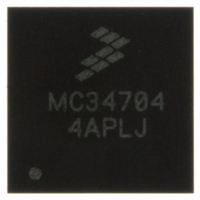
MC34704AEP Freescale Semiconductor, MC34704AEP Datasheet - Page 18

MC34704AEP
Manufacturer Part Number
MC34704AEP
Description
IC POWER MANAGEMENT 56-QFN
Manufacturer
Freescale Semiconductor
Datasheet
1.MC34704BEPR2.pdf
(54 pages)
Specifications of MC34704AEP
Applications
Processor
Current - Supply
86mA
Voltage - Supply
2.7 V ~ 5.5 V
Operating Temperature
-20°C ~ 85°C
Mounting Type
Surface Mount
Package / Case
56-QFN
Output Voltage
5 V
Input Voltage
2.7 V to 5.5 V
Switching Frequency
750 KHz to 2 MHz
Mounting Style
SMD/SMT
Number Of Outputs
8
Lead Free Status / RoHS Status
Lead free / RoHS Compliant
REG1 REGULATED OUTPUT VOLTAGE PIN
(VOUT1) (34704A ONLY)
output filter as close to the pin as possible.
REG1 BOOTSTRAP CAPACITOR INPUT PIN (BT1)
to enhance the gate of the Switch Power MOSFET.
I
I
POWER RESET OUTPUT SIGNAL
(MICROPROCESSOR RESET) (RST)
external resistor to a supply voltage like V
REG7 COMPENSATION NETWORK CONNECTION
(COMP7)
REG7 RESISTOR FEEDBACK NETWORK
REFERENCE VOLTAGE (VREF7) (34704A ONLY)
divider.
REG7 VOLTAGE FEEDBACK INPUT FOR
VOLTAGE REGULATION/PROGRAMMING (FB7)
(34704A ONLY)
REG7 EXTERNAL POWER MOSFET GATE DRIVE
(DRV7) (34704A ONLY)
REG7 OUTPUT VOLTAGE RETURN PIN (VOUT7)
(34704A ONLY)
REG6 VOLTAGE FEEDBACK INPUT FOR
VOLTAGE REGULATION/PROGRAMMING (FB6)
(34704A ONLY)
REG6 BOOTSTRAP CAPACITOR INPUT PIN (BT6)
(34704A ONLY)
to enhance the gate of the Synchronous Power MOSFET.
18
34704
FUNCTIONAL DESCRIPTION
FUNCTIONAL PIN DESCRIPTION
2
2
C SERIAL INTERFACE CLOCK INPUT (SCL)
C SERIAL INTERFACE DATA INPUT (SDA)
Connect this pin directly to the load directly and to the
Connect a 1.0 μF capacitor between this pin and SW1 pin
I
I
This is an open drain output and must be pulled up by an
REG7 compensation network connection.
Connect this pin to the bottom of the feedback resistor
Connect the feedback resistor divider to this pin.
REG7 external Power MOSFET gate drive.
This is the discharge path of REG7 output voltage.
Connect the feedback resistor divider to this pin.
Connect a 0.01 μF capacitor between this pin and SW6 pin
2
2
C serial interface clock input.
C serial interface data input
IN
.
REG6 SWITCHING NODE (SW6) (34704A ONLY)
pin.
REG6 REGULATED OUTPUT VOLTAGE PIN
(VOUT6) (34704A ONLY)
output filter as close to the pin as possible.
ANALOG GROUND (AGND)
BATTERY VOLTAGE CONNECTION (VIN)
operate properly.
INTERNAL SUPPLY VOLTAGE (VDDI)
between this pin and GND.
BATTERY DETECTION (LION)
battery.
DUAL FUNCTION IC TURN ON/OFF (ONOFF)
connected to a mechanical switch to turn the power On or Off.
REG2 BOOST STAGE BOOTSTRAP CAPACITOR
INPUT PIN (BT2U)
pin to enhance the gate of the Switch Power MOSFET.
REG2 COMPENSATION NETWORK CONNECTION
(COMP2)
REG2 VOLTAGE FEEDBACK INPUT FOR
VOLTAGE REGULATION/PROGRAMMING (FB2)
REG2 BUCK STAGE BOOTSTRAP CAPACITOR
INPUT PIN (BT2D)
pin to enhance the gate of the Switch Power MOSFET.
REG2 POWER SUPPLY INPUT VOLTAGE (PVIN2)
FET. Input decoupling /filtering is required for proper REG2
operation.
The inductor is connected between this pin and the VIN
Connect this pin directly to the load directly and to the
Analog ground of the IC.
Input decoupling /filtering is required for the device to
Connect a 1.0 μF low ESR decoupling filter capacitor
Pull this pin high to VIN to indicate a connection to a Li-Ion
This is a hardware enable/disable for the 34704. It can be
Connect a 1.0 μF capacitor between this pin and SW2U
REG2 compensation network connection.
Connect the feedback resistor divider to this pin.
Connect a 1.0 μF capacitor between this pin and SW2D
This is the connection to the drain of the high side switch
Analog Integrated Circuit Device Data
Freescale Semiconductor


