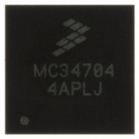
MC34704AEP Freescale Semiconductor, MC34704AEP Datasheet - Page 28

MC34704AEP
Manufacturer Part Number
MC34704AEP
Description
IC POWER MANAGEMENT 56-QFN
Manufacturer
Freescale Semiconductor
Datasheet
1.MC34704BEPR2.pdf
(54 pages)
Specifications of MC34704AEP
Applications
Processor
Current - Supply
86mA
Voltage - Supply
2.7 V ~ 5.5 V
Operating Temperature
-20°C ~ 85°C
Mounting Type
Surface Mount
Package / Case
56-QFN
Output Voltage
5 V
Input Voltage
2.7 V to 5.5 V
Switching Frequency
750 KHz to 2 MHz
Mounting Style
SMD/SMT
Number Of Outputs
8
Lead Free Status / RoHS Status
Lead free / RoHS Compliant
POWER-UP SEQUENCE
connection or a Power On signal through the ONOFF pin.
grouped based on their function and how they relate to each
28
34704
FUNCTIONAL DEVICE OPERATION
OPERATIONAL MODES
10. When REG1 is in regulation, it will be used to supply
12. REG2 is enabled, then when REG2 is in regulation.
13. REG4 is enabled, then when REG4 is in regulation.
14. I
15. 34704 will de-assert the RST signal to indicate a
16. The microprocessor then takes over and can enable
11. REG3 is enabled, then when REG3 is in regulation.
1. Battery initially connected to VIN.
2. LION pin is used to determine if a battery is being used
3. At initial power up from a cold start like the above with
4. After the cold start or battery insertion power up,
5. The input battery UVLO signal de-asserts if the input
6. REG1 VG starts up in peak detect PFM and REG1 VG
7. V
8. When REG1 VG output rises high enough such that
9. REG1 PWM control loop can take over control of
Following is the power up sequence from a battery
For power sequencing needs, the different regulators are
(High for Li-Ion battery).
the battery first connected, the status of the ONOFF
pin is ignored and 34704 moves forward to step (5).
activity on the ONOFF pin is used to determine if the
device is enabled or disabled. If the device is disabled,
then nothing happens. If the device is enabled then,
34704 moves forward to step (5).
voltage is above the UVLO rising threshold.
output starts rising.
V
and all internal circuitry can be enabled. I
communication will remain disabled for normal power
up sequence. The values of the FREQ and SS pins are
read at this point.
REG1 output once the VG voltage reaches a certain
threshold set internally.
the Power MOSFET gate voltage for all of the other
regulators except REG7.
supplies are up.
“Power Good” after 10 ms of wait time. This output will
be connected to the reset pin of the microprocessor.
REG1 VOUT1 and REG5 through REG8. The
processor needs to send a command for REG8 mode
of operation. The processor can also change REG5-8
soft start time before enabling them. The processor can
also power down the system with an ALLOFF
command.
2
DDI
DDI
C communication is enabled now since the processor
output voltage will start tracking REG1 VG output.
voltage is in regulation a POR signal is released
FUNCTIONAL DEVICE OPERATION
2
C
OPERATIONAL MODES
other and the entire system. This makes power sequencing
control a much easier task for the user where most of the
group internal sequencing in now handled by the PMIC. All
the processor has to do is to command the group and not
each regulator.
• GrpA: Includes REG1 (VOUT1)
• GrpB: Includes REG2, REG3, and REG4
• GrpC: Includes REG5, REG6, and REG7
• GrpD: Includes REG8
• GrpE: This is a special group. It includes REG5 when
SHUTDOWN SEQUENCES
• Processor can disable VOUT1 (GrpA) at any point it
• Processor can disable REG8 (GrpD) at any point it desires
• Processor can disable REG5 (GrpE) at any point it desires
• Processor can shutdown GrpC according to the power
• If any regulator in GrpC is shutting down due to a fault, the
• If any regulator in GrpB is shutting down due to a fault, the
• Processor can shutdown the 34704 by sending an
• The previous shutdown event can also happen through the
• During battery depletion and when the input voltage
The regulators groups are as follows:
GrpC/E power sequencing option#1 is chosen
desires
if sequencing option#1 is picked
sequencing options 1, 2, 3, or 4 (see section
Interface”)
other regulators in GrpC will also shutdown by following
the GrpC power sequencing options 1, 2, 3, or 4 (see
section
other regulators in GrpB will also shutdown by following
the processor supplies shutdown sequence. Then, GrpA,
GrpC, GrpD, and GrpE (if applicable) will simultaneously
shutdown keeping any sequencing within each group as
necessary. VG will stay alive to perform a power up retry
for GrpB but only for one time. If the power up cycle is
successful, then normal operation is back. If the fault
returns, then the shutdown sequence is repeated and then
VG shuts down
“ALLOFF” command, then GrpA, GrpC, GrpD, and GrpE
(if applicable) will simultaneously shutdown keeping any
sequencing within each group as necessary. Then, GrpB
will shutdown according to the processor supply shutdown
sequence. Then, VG will shut down.
ONOFF pin by pressing and holding the pin for a time
period (programmable through I
passes the UVLO falling threshold, all of the outputs will be
disabled without honouring the power down sequence
This is to guarantee that the outputs are off and battery is
not depleted further.
“I
2
C User
Interface”)
Analog Integrated Circuit Device Data
2
Freescale Semiconductor
C with a default of 1sec)
“I
2
C User


