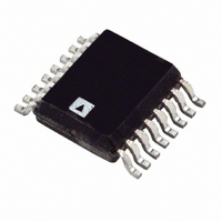
ADT7470ARQZ Analog Devices Inc, ADT7470ARQZ Datasheet - Page 10

ADT7470ARQZ
Manufacturer Part Number
ADT7470ARQZ
Description
IC SENSOR TEMP FAN CTRLR 16QSOP
Manufacturer
Analog Devices Inc
Datasheet
1.ADT7470ARQZ.pdf
(40 pages)
Specifications of ADT7470ARQZ
Function
Fan Control, Temp Monitor
Topology
ADC, Comparator, Fan Speed Control, Register Bank
Sensor Type
External
Sensing Temperature
External Sensor
Output Type
I²C™
Output Alarm
No
Output Fan
Yes
Voltage - Supply
3 V ~ 5.5 V
Operating Temperature
-40°C ~ 125°C
Mounting Type
Surface Mount
Package / Case
16-QSOP
Ic Output Type
Digital
Sensing Accuracy Range
± 12%
Supply Current
500µA
Supply Voltage Range
3V To 5.5V
Sensor Case Style
QSOP
No. Of Pins
16
Msl
MSL 3 - 168 Hours
Termination Type
SMD
Filter Terminals
SMD
Rohs Compliant
Yes
Accuracy %
12%
Lead Free Status / RoHS Status
Lead free / RoHS Compliant
For Use With
EVAL-ADT7470EBZ - BOARD EVALUATION FOR ADT7470
Lead Free Status / RoHS Status
Lead free / RoHS Compliant, Lead free / RoHS Compliant
Available stocks
Company
Part Number
Manufacturer
Quantity
Price
Company:
Part Number:
ADT7470ARQZ
Manufacturer:
AVX
Quantity:
7 600
Part Number:
ADT7470ARQZ
Manufacturer:
ADI/亚德诺
Quantity:
20 000
Part Number:
ADT7470ARQZ-REEL7
Manufacturer:
ADI/亚德诺
Quantity:
20 000
ADT7470
Any number of bytes of data can be transferred over the serial
bus in one operation. However, it is not possible to mix read
and write in one operation, because the type of operation is
determined at the beginning and subsequently cannot be
changed without starting a new operation.
In the ADT7470, write operations contain either one or two
bytes, and read operations contain one byte and perform the
following functions.
during the low period before the 10th clock pulse, then
high during the 10th clock pulse to assert a stop condition.
SDA
SCL
SDA
SCL
START BY
START BY
MASTER
MASTER
SDA
SCL
START BY
MASTER
1
0
1
0
1
0
Figure 7. Writing a Register Address to the Address Pointer Register, Then Writing Data to the Selected Register
1
1
1
0
0
SERIAL BUS ADDRESS
SERIAL BUS ADDRESS
0
SERIAL BUS ADDRESS
1
1
FRAME 1
FRAME 1
BYTE
BYTE
1
FRAME 1
BYTE
1
1
1
SDA (CONTINUED)
SCL (CONTINUED)
Figure 9. Reading Data from a Previously Selected Register
A1
A1
Figure 8. Writing to the Address Pointer Register Only
A1
A0
A0
A0
R/W
R/W
R/W
ADT7470
ACK. BY
ADT7470
ACK. BY
Rev. C | Page 10 of 40
ADT7470
ACK. BY
9
9
D7
1
9
D7
D7
1
1
D6
D7
1
D6
D6
To write data to one of the device data registers or read data
from it, the address pointer register must be set so that the
correct data register is addressed. Then data can be written into
that register or read from it. The first byte of a write operation
always contains an address that is stored in the address pointer
register. If data is to be written to the device, the write operation
contains a second data byte that is written to the register selected
by the address pointer register.
This is illustrated in Figure 7. The device address is sent over the
bus followed by R/ W set to 0. This is followed by two data bytes.
D6
D5
ADDRESS POINTER REGISTER BYTE
D5
D5
ADDRESS POINTER REGISTER BYTE
D5
D4
DATA BYTE FROM
FRAME 3
D4
D4
DATA
BYTE
D3
D4
FRAME 2
ADT7470
FRAME 2
D3
D3
FRAME 2
D3
D2
D2
D2
D2
D1
D1
D1
D0
D1
ADT7470
ACK. BY
D0
D0
BY MASTER
D0
NO ACK.
9
ADT7470
ACK. BY
ADT7470
ACK. BY
9
9
9
STOP BY
MASTER
STOP BY
MASTER
STOP BY
MASTER


