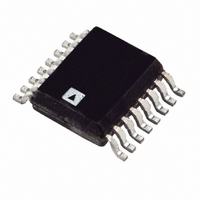
ADT7470ARQZ Analog Devices Inc, ADT7470ARQZ Datasheet - Page 9

ADT7470ARQZ
Manufacturer Part Number
ADT7470ARQZ
Description
IC SENSOR TEMP FAN CTRLR 16QSOP
Manufacturer
Analog Devices Inc
Datasheet
1.ADT7470ARQZ.pdf
(40 pages)
Specifications of ADT7470ARQZ
Function
Fan Control, Temp Monitor
Topology
ADC, Comparator, Fan Speed Control, Register Bank
Sensor Type
External
Sensing Temperature
External Sensor
Output Type
I²C™
Output Alarm
No
Output Fan
Yes
Voltage - Supply
3 V ~ 5.5 V
Operating Temperature
-40°C ~ 125°C
Mounting Type
Surface Mount
Package / Case
16-QSOP
Ic Output Type
Digital
Sensing Accuracy Range
± 12%
Supply Current
500µA
Supply Voltage Range
3V To 5.5V
Sensor Case Style
QSOP
No. Of Pins
16
Msl
MSL 3 - 168 Hours
Termination Type
SMD
Filter Terminals
SMD
Rohs Compliant
Yes
Accuracy %
12%
Lead Free Status / RoHS Status
Lead free / RoHS Compliant
For Use With
EVAL-ADT7470EBZ - BOARD EVALUATION FOR ADT7470
Lead Free Status / RoHS Status
Lead free / RoHS Compliant, Lead free / RoHS Compliant
Available stocks
Company
Part Number
Manufacturer
Quantity
Price
Company:
Part Number:
ADT7470ARQZ
Manufacturer:
AVX
Quantity:
7 600
Part Number:
ADT7470ARQZ
Manufacturer:
ADI/亚德诺
Quantity:
20 000
Part Number:
ADT7470ARQZ-REEL7
Manufacturer:
ADI/亚德诺
Quantity:
20 000
SMBUS/I
Control of the ADT7470 is carried out using the serial system
management bus (SMBus). This interface is fully compatible
with SMBus 2.0 electrical specifications and meets 400 pF bus
capacitance requirements. The device also supports fast I
(400 kHz max). The ADT7470 is connected to the bus as a slave
device under the control of a master controller or service
processor.
ADDRESS SELECTION
The ADT7470 has a 7-bit serial bus address. When the device
is powered up with Pin 11 (ADDR) high, the ADT7470 has an
SMBus address of 010 1111 or 0x5E (left-justified). Because the
address is 7 bits, it can be left- or right-justified; this determines
whether the address reads as 0x5x or 0x2x. Pin 11 can be left
floating or tied low for other addressing options, as shown in
Table 5. See also Figure 4, Figure 5, and Figure 6.
Table 5. ADT7470 Address Select Mode
Pin 11 (ADDR) State
High (10 kΩ to V
Low (10 kΩ to GND)
Floating (no pull-up)
Figure 5. SMBus Address = 0x58 or 0x2C (Pin 11 = 0)
Figure 4. SMBus Address = 0x5E or 0x2F (Pin 11 = 1)
2
2
3
4
5
6
7
8
1
1
2
3
4
5
6
7
8
C SERIAL INTERFACE
CC
)
ADT7470
ADT7470
Address
010 1111 (0x5E left-justified or
0x2F right-justified)
010 1100 (0x58 left-justified or
0x2C right-justified)
010 1110 (0x5C left-justified or
0x2E right-justified)
15
14
13
12
11
10
16
9
15
14
13
12
11
10
16
9
ADDR
ADDR
V
CC
10kΩ
TYP
10kΩ
TYP
2
C
Rev. C | Page 9 of 40
The device address is sampled and latched on the first valid
SMBus transaction, so any additional attempted addressing
changes have no immediate effect. The facility to make
hardwired changes to the SMBus slave address allows the user
to avoid conflicts with other devices sharing the same serial bus,
for example, if more than one ADT7470 is used in a system.
SERIAL BUS PROTOCOL
The serial bus protocol operates as follows:
1.
2.
3.
The master initiates data transfer by establishing a start
condition, defined as a high-to-low transition on the serial
data line, SDA, while the serial clock line, SCL, remains
high. This indicates that an address/data stream follows.
All slave peripherals connected to the serial bus respond
to the start condition, and shift in the next 8 bits, consist-
ing of a 7-bit address (MSB first) and an R/ W bit. This
determines the direction of the data transfer, that is,
whether data is written to or read from the slave device.
The peripheral whose address corresponds to the transmit-
ted address responds by pulling the data line low during
the low period before the 9th clock pulse, known as the
acknowledge bit. All other devices on the bus now remain
idle while the selected device waits for data to be read from
or written to it. If the R/ W bit is 0, the master writes to the
slave device. If the R/ W bit is 1, the master reads from the
slave device.
Data is sent over the serial bus in sequences of 9 clock pulses:
8 bits of data followed by an acknowledge bit from the slave
device. Transitions on the data line must occur during the
low period of the clock signal and remain stable during the
high period. This is because a low-to-high transition when
the clock is high might be interpreted as a stop signal. The
number of data bytes that can be transmitted over the serial
bus in a single read or write operation is limited only by
what the master and slave devices can handle.
After all data bytes are read or written, stop conditions
are established. In write mode, the master pulls the data
line high during the 10th clock pulse to assert a stop
condition. In read mode, the master device overrides
the acknowledge bit by pulling the data line high during
the low period before the 9th clock pulse. This is known as
No Acknowledge. The master then takes the data line low
Figure 6. SMBus Address = 0x5C or 0x2E (Pin 11 = Floating)
2
3
4
5
6
7
8
1
ADT7470
16
15
14
13
12
11
10
9
ADDR
ADT7470


