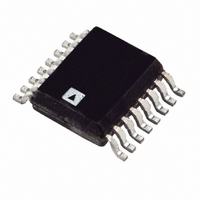
ADT7470ARQZ Analog Devices Inc, ADT7470ARQZ Datasheet - Page 30

ADT7470ARQZ
Manufacturer Part Number
ADT7470ARQZ
Description
IC SENSOR TEMP FAN CTRLR 16QSOP
Manufacturer
Analog Devices Inc
Datasheet
1.ADT7470ARQZ.pdf
(40 pages)
Specifications of ADT7470ARQZ
Function
Fan Control, Temp Monitor
Topology
ADC, Comparator, Fan Speed Control, Register Bank
Sensor Type
External
Sensing Temperature
External Sensor
Output Type
I²C™
Output Alarm
No
Output Fan
Yes
Voltage - Supply
3 V ~ 5.5 V
Operating Temperature
-40°C ~ 125°C
Mounting Type
Surface Mount
Package / Case
16-QSOP
Ic Output Type
Digital
Sensing Accuracy Range
± 12%
Supply Current
500µA
Supply Voltage Range
3V To 5.5V
Sensor Case Style
QSOP
No. Of Pins
16
Msl
MSL 3 - 168 Hours
Termination Type
SMD
Filter Terminals
SMD
Rohs Compliant
Yes
Accuracy %
12%
Lead Free Status / RoHS Status
Lead free / RoHS Compliant
For Use With
EVAL-ADT7470EBZ - BOARD EVALUATION FOR ADT7470
Lead Free Status / RoHS Status
Lead free / RoHS Compliant, Lead free / RoHS Compliant
Available stocks
Company
Part Number
Manufacturer
Quantity
Price
Company:
Part Number:
ADT7470ARQZ
Manufacturer:
AVX
Quantity:
7 600
Part Number:
ADT7470ARQZ
Manufacturer:
ADI/亚德诺
Quantity:
20 000
Part Number:
ADT7470ARQZ-REEL7
Manufacturer:
ADI/亚德诺
Quantity:
20 000
ADT7470
Table 27. Register 0x38 to Register 0x3B. PWM Max Duty Cycle Registers (Power-On Default = 0xFF).
Register Address
0x38
0x39
0x3A
0x3B
Table 28. Register 0x3D. Device ID Register (Power-On Default = 0x70).
Register Address
0x3D
The device ID register contains the ADT7470 device ID value as a means of identifying the part over the bus.
Table 29. Register 0x3E. Company ID Register (Power-On Default = 0x41).
Register Address
0x3E
The company ID register contains 0x41, the manufacturer ID number representative of the Analog Devices, Inc. product.
Table 30. Register 0x3F. Revision Register (Power-On Default = 0x02).
Register Address
0x3F
The revision register contains the revision number of the ADT7470.
Table 31. Register 0x40. Configuration Register 1 (Power-On Default = 0x01).
Bit Name
[0] STRT
[1] Reserved
[2] Reserved
[3] TODIS
[4] LOCK
[5] FST_TCH
[6] HF_LF
[7] T05_STB
Read/Write
Read/Write
Read/Write
Read/Write
Read/Write
Read/Write
Read only
Read/Write
Read only
Read/Write
Read only
Read/Write
Read/Write
Read/Write
Read/Write
Read/Write
Read/Write
Write Once
Read/Write
Read/Write
Description
PWM1 max duty cycle: PWM1 Min duty cycle value (register 0x6A) to 100% duty cycle.
PWM2 max duty cycle: PWM2 Min duty cycle value (register 0x6B) to 100% duty cycle.
PWM3 max duty cycle: PWM3 Min duty cycle value (register 0x6C) to 100% duty cycle.
PWM4 max duty cycle: PWM4 Min duty cycle value (register 0x6D) to 100% duty cycle.
Description
Device ID.
Description
Company ID.
Description
Revision Register.
Description
Logic 1 enables monitoring and PWM control outputs based on the limit settings
programmed.
Logic 0 disables monitoring and PWM control based on the default power-up limit settings.
The limit values programmed are preserved even if a Logic 0 is written to this bit and the
default settings are enabled.
Reserved. Write 0 to this bit.
Reserved. Write 0 to this bit.
Writing a 1 disables SMBus timeout.
Once this bit is set, all lockable registers become read-only and cannot be modified until the
ADT7470 is powered down and powered up again.
Enable Fast Tach measurement.
0 = Tach measurement rate is 1 measurement per second
1= Tach measurement rate is 1 measurement every 250ms
This bit switches between high frequency and low frequency fan drive.
0 (default) = high frequency fan drive (1.4 kHz or 22.5 kHz. See Configuration Register 2,
Register 0x74, Bits [6:4]) in Table 44.
1 = low frequency fandrive (frequency determined by Configuration Register 2, Register 0x74,
Bits[6:4]) in Table 44.
Select configuration for Pin 13.
0 (default) =FULL SPEED input.
1 = TMP05 start pulse output.
Rev. C | Page 30 of 40


