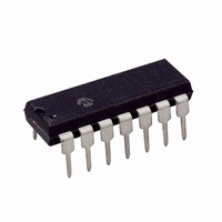
TC9402CPD Microchip Technology, TC9402CPD Datasheet - Page 10

TC9402CPD
Manufacturer Part Number
TC9402CPD
Description
IC V-FREQ/FREQ-V CONV 14DIP
Manufacturer
Microchip Technology
Type
Volt to Freq & Freq to Voltr
Specifications of TC9402CPD
Package / Case
14-DIP (0.300", 7.62mm)
Frequency - Max
100kHz
Full Scale
±100ppm/°C
Linearity
±0.25%
Mounting Type
Through Hole
Supply Voltage (max)
15 V
Supply Voltage (min)
8 V
Maximum Operating Temperature
70 C
Minimum Operating Temperature
0 C
Dual Supply Voltage
+/- 5 V
Full Scale Frequency
100 KHz
Linearity Error
+/- 0.5 % FSR
Maximum Dual Supply Voltage
+/- 7.5 V
Minimum Dual Supply Voltage
+/- 4 V
Mounting Style
Through Hole
Operating Supply Voltage
9 V or 12 V
Frequency
100kHz
Full Scale Range
1Hz To 100kHz
Linearity %
0.25%
Supply Voltage Range
± 4V To ± 7.5V
Digital Ic Case Style
DIP
No. Of Pins
14
Frequency Max
100kHz
Rohs Compliant
Yes
Lead Free Status / RoHS Status
Lead free / RoHS Compliant
Lead Free Status / RoHS Status
Lead free / RoHS Compliant, Lead free / RoHS Compliant
Other names
158-1142
158-1142
158-1142
TC9400/9401/9402
4.9
A reference voltage from either a precision source, or
the V
TC9400 is dependent on the voltage regulation and
temperature characteristics of the reference circuitry.
Since the TC9400 is a charge balancing V/F converter,
the reference current will be equal to the input current.
For this reason, the DC impedance of the reference
voltage source must be kept low enough to prevent lin-
earity errors. For linearity of 0.01%, a reference imped-
ance of 200W or less is recommended. A 0.1 μF
bypass capacitor should be connected from V
ground.
4.10
The charging current for C
pin. When the op amp output reaches the threshold
level, this pin is internally connected to the reference
voltage and a charge, equal to V
from the integrator capacitor. After about 3μsec, this pin
is internally connected to the summing junction of the
op amp to discharge C
ing ensures that the reference voltage is not directly
applied to the summing junction.
DS21483C-page 10
SS
supply is applied to this pin. Accuracy of the
V
V
REF
REF
Out
REF
. Break-before-make switch-
REF
is supplied through this
REF
x C
REF
, is removed
REF
to
5.0
5.1
The output frequency (F
input voltage (V
EQUATION 5-1:
5.2
5.2.1
The value of this component is chosen to give a full
scale input current of approximately 10 μA:
EQUATION 5-2:
EQUATION 5-3:
Note that the value is an approximation and the exact
relationship is defined by the transfer equation. In prac-
tice, the value of R
obtain full scale frequency at V
Section 5.3 “Adjustment Procedure”, Adjustment
Procedure). Metal film resistors with 1% tolerance or
better are recommended for high accuracy applications
because of their thermal stability and low noise gener-
ation.
5.2.2
The exact value is not critical but is related to C
the relationship:
Improved stability and linearity are obtained when
C
although mica and ceramic devices can be used in
applications where their temperature limits are not
exceeded. Locate as close as possible to Pins 12
and 13.
INT
≤ 4C
Frequency Out =
VOLTAGE-TO-FREQUENCY
(V/F) CONVERTER DESIGN
INFORMATION
Input/Output Relationships
External Component Selection
REF
R
C
. Low leakage types are recommended,
IN
INT
3C
R
IN
IN
) by the transfer equation:
R
REF
IN
≅
IN
≅
≤ C
V
typically would be trimmed to
10 μA
© 2006 Microchip Technology Inc.
IN
10V
OUT
R
V
INT
FULLSCALE
IN
IN
10 μA
) is related to the analog
≤ 10C
, x
= 1 MΩ
(V
REF
IN
REF
)(V
full scale (see
1
REF
)
REF
by


