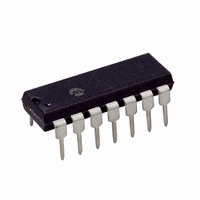
TC9402CPD Microchip Technology, TC9402CPD Datasheet - Page 9

TC9402CPD
Manufacturer Part Number
TC9402CPD
Description
IC V-FREQ/FREQ-V CONV 14DIP
Manufacturer
Microchip Technology
Type
Volt to Freq & Freq to Voltr
Specifications of TC9402CPD
Package / Case
14-DIP (0.300", 7.62mm)
Frequency - Max
100kHz
Full Scale
±100ppm/°C
Linearity
±0.25%
Mounting Type
Through Hole
Supply Voltage (max)
15 V
Supply Voltage (min)
8 V
Maximum Operating Temperature
70 C
Minimum Operating Temperature
0 C
Dual Supply Voltage
+/- 5 V
Full Scale Frequency
100 KHz
Linearity Error
+/- 0.5 % FSR
Maximum Dual Supply Voltage
+/- 7.5 V
Minimum Dual Supply Voltage
+/- 4 V
Mounting Style
Through Hole
Operating Supply Voltage
9 V or 12 V
Frequency
100kHz
Full Scale Range
1Hz To 100kHz
Linearity %
0.25%
Supply Voltage Range
± 4V To ± 7.5V
Digital Ic Case Style
DIP
No. Of Pins
14
Frequency Max
100kHz
Rohs Compliant
Yes
Lead Free Status / RoHS Status
Lead free / RoHS Compliant
Lead Free Status / RoHS Status
Lead free / RoHS Compliant, Lead free / RoHS Compliant
Other names
158-1142
158-1142
158-1142
4.0
4.1
In the V/F mode, this input is connected to the AMPLI-
FIER OUT output (Pin 12) and triggers a 3μsec pulse
when the input voltage passes through its threshold. In
the F/V mode, the input frequency is applied to this
input.
The nominal threshold of the detector is half way
between the power supplies, or (V
mV. The TC9400’s charge balancing V/F technique is
not dependent on a precision comparator threshold,
because the threshold only sets the lower limit of the op
amp output. The op amp’s peak-to-peak output swing,
which determines the frequency, is only influenced by
external capacitors and by V
FIGURE 4-1:
4.4
The sources of both the FREQ/2 OUT and the PULSE
FREQ OUT are connected to this pin. An output level
swing from the drain voltage to ground, or to the V
supply, may be obtained by connecting this pin to the
appropriate point.
4.5
An external resistor, connected to V
point for the TC9400. Specifications for the TC9400 are
based on R
noted.
Increasing the maximum frequency of the TC9400
beyond 100 kHz is limited by the pulse width of the
pulse output (typically 3μsec). Reducing R
decrease the pulse width and increase the maximum
operating frequency, but linearity errors will also
increase. R
typically produce a maximum full scale frequency of
500 kHz.
© 2006 Microchip Technology Inc.
PIN FUNCTIONS
Threshold Detector Input
Output Common
R
F
Amp Out
OUT
F
BIAS
BIAS
OUT
BIAS
/2
Notes: 1. To adjust F
can be reduced to 20 kΩ, which will
= 100 kΩ ±10%, unless otherwise
Output Waveforms
2. To adjust F
3. To increase F
4. For high performance applications, use high stability components for R
resistors and glass capacitors). Also, separate output ground (Pin 9) from input ground (Pin 6).
REF
1/f
.
MIN
MAX
DD
OUT
SS
, set V
3msec
Typ.
, set V
+ V
, sets the bias
MAX
IN
SS
IN
to 100 kHz, change C
= 10 mV and adjust the 50 kW offset for 10 Hz output.
)/2 ±400
= 10V and adjust R
BIAS
will
SS
IN
REF
4.2
This output is an open drain N-channel FET, which
provides a pulse waveform whose frequency is propor-
tional to the input voltage. This output requires a pull-
up resistor and interfaces directly with MOS, CMOS,
and TTL logic (see Figure 4-1).
4.3
This output is an open drain N-channel FET, which pro-
vides a square wave one-half the frequency of the
pulse frequency output. The FREQ/2 OUT output will
change state on the rising edge of PULSE FREQ OUT.
This output requires a pull-up resistor and interfaces
directly with MOS, CMOS, and TTL logic.
or V
4.6
This pin is the output stage of the operational amplifier.
During V/F operation, a negative going ramp signal is
available at this pin. In the F/V mode, a voltage
proportional to the frequency input is generated.
4.7
This pin is the non-inverting input of the operational
amplifier. The low frequency set point is determined by
adjusting the voltage at this pin.
4.8
The inverting input of the operational amplifier and the
summing junction when connected in the V/F mode. An
input current of 10 μA is specified, but an over range
current up to 50 μA can be used without detrimental
effect to the circuit operation. I
junction of an operational amplifier. Voltage sources
cannot be attached directly, but must be buffered by
external resistors.
to 2pF and C
REF
TC9400/9401/9402
for 10 kHz output.
Pulse Freq Out
Freq/2 Out
Amplifier Out
Zero Adjust
I
IN
INT
to 75 pF.
IN
, C
REF
, V
REF
IN
connects the summing
V
0V
(metal film
REF
DS21483C-page 9
C
C
REF
INT


