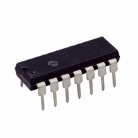
TC9402CPD Microchip Technology, TC9402CPD Datasheet - Page 11

TC9402CPD
Manufacturer Part Number
TC9402CPD
Description
IC V-FREQ/FREQ-V CONV 14DIP
Manufacturer
Microchip Technology
Type
Volt to Freq & Freq to Voltr
Specifications of TC9402CPD
Package / Case
14-DIP (0.300", 7.62mm)
Frequency - Max
100kHz
Full Scale
±100ppm/°C
Linearity
±0.25%
Mounting Type
Through Hole
Supply Voltage (max)
15 V
Supply Voltage (min)
8 V
Maximum Operating Temperature
70 C
Minimum Operating Temperature
0 C
Dual Supply Voltage
+/- 5 V
Full Scale Frequency
100 KHz
Linearity Error
+/- 0.5 % FSR
Maximum Dual Supply Voltage
+/- 7.5 V
Minimum Dual Supply Voltage
+/- 4 V
Mounting Style
Through Hole
Operating Supply Voltage
9 V or 12 V
Frequency
100kHz
Full Scale Range
1Hz To 100kHz
Linearity %
0.25%
Supply Voltage Range
± 4V To ± 7.5V
Digital Ic Case Style
DIP
No. Of Pins
14
Frequency Max
100kHz
Rohs Compliant
Yes
Lead Free Status / RoHS Status
Lead free / RoHS Compliant
Lead Free Status / RoHS Status
Lead free / RoHS Compliant, Lead free / RoHS Compliant
Other names
158-1142
158-1142
158-1142
5.2.3
The exact value is not critical and may be used to trim
the full scale frequency (see Section 7.1 “Input/Out-
put Relationships”, Input/Output Relationships).
Glass film or air trimmer capacitors are recommended
because of their stability and low leakage. Locate as
close as possible to Pins 5 and 3 (see Figure ).
FIGURE 5-1:
V
5.2.4
Power supplies of ±5V are recommended. For high
accuracy requirements, 0.05% line and load regulation
and 0.1 μF disc decoupling capacitors, located near the
pins, are recommended.
© 2006 Microchip Technology Inc.
REF
500
400
300
200
100
C
V
0
DD
REF
, V
-1
SS
-2
Recommended C
10 kHz
V
-3
100 kHz
REF
-4
(V)
V
V
R
V
T
-5
DD
SS
IN
A
IN
= +25°C
= +10V
= 1MW
= -5V
= +5V
-6
REF
-7
vs.
5.3
Figure 3-1 shows a circuit for trimming the zero loca-
tion. Full scale may be trimmed by adjusting R
or C
scale frequency is as follows:
1.
2.
If adjustments are performed in this order, there should
be no interaction and they should not have to be
repeated.
5.4
A TC9400, which operates from a single 12 to 15V vari-
able power source, is shown in Figure 5-2. This circuit
uses two Zener diodes to set stable biasing levels for
the TC9400. The Zener diodes also provide the refer-
ence voltage, so the output impedance and tempera-
ture coefficient of the Zeners will directly affect power
supply rejection and temperature performance. Full
scale adjustment is accomplished by trimming the input
current.
Trimming the reference voltage is not recommended
for high accuracy applications unless an op amp is
used as a buffer, because the TC9400 requires a low-
impedance reference (see Section 4.9 “VREF”, V
pin description, for more information).
The circuit of Figure 5-2 will directly interface with
CMOS logic operating at 12V to 15V. TTL or 5V CMOS
logic can be accommodated by connecting the output
pull-up resistors to the +5V supply. An optoisolator can
also be used if an isolated output is required; also, see
Figure 5-3.
Set V
to obtain a 10 Hz output frequency.
Set V
to obtain a 10 kHz output frequency.
REF
TC9400/9401/9402
. Recommended procedure for a 10 kHz full
Adjustment Procedure
Improved Single Supply V/F
Converter Operation
IN
IN
to 10V and trim either R
to 10 mV and trim the zero adjust circuit
IN
DS21483C-page 11
, V
REF
, or C
IN
, V
REF
REF
REF
,


