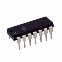
TC9402CPD Microchip Technology, TC9402CPD Datasheet - Page 15

TC9402CPD
Manufacturer Part Number
TC9402CPD
Description
IC V-FREQ/FREQ-V CONV 14DIP
Manufacturer
Microchip Technology
Type
Volt to Freq & Freq to Voltr
Specifications of TC9402CPD
Package / Case
14-DIP (0.300", 7.62mm)
Frequency - Max
100kHz
Full Scale
±100ppm/°C
Linearity
±0.25%
Mounting Type
Through Hole
Supply Voltage (max)
15 V
Supply Voltage (min)
8 V
Maximum Operating Temperature
70 C
Minimum Operating Temperature
0 C
Dual Supply Voltage
+/- 5 V
Full Scale Frequency
100 KHz
Linearity Error
+/- 0.5 % FSR
Maximum Dual Supply Voltage
+/- 7.5 V
Minimum Dual Supply Voltage
+/- 4 V
Mounting Style
Through Hole
Operating Supply Voltage
9 V or 12 V
Frequency
100kHz
Full Scale Range
1Hz To 100kHz
Linearity %
0.25%
Supply Voltage Range
± 4V To ± 7.5V
Digital Ic Case Style
DIP
No. Of Pins
14
Frequency Max
100kHz
Rohs Compliant
Yes
Lead Free Status / RoHS Status
Lead free / RoHS Compliant
Lead Free Status / RoHS Status
Lead free / RoHS Compliant, Lead free / RoHS Compliant
Other names
158-1142
158-1142
158-1142
7.0
7.1
The output voltage is related to the input frequency
(F
EQUATION 7-1:
The response time to a change in F
C
proportional to C
C
to 100 μF are perfectly acceptable for low frequencies.
When the TC9400 is used in the Single Supply mode,
V
and Pin 2.
FIGURE 7-1:
© 2006 Microchip Technology Inc.
REF
INT
INT
IN
Frequency
) by the transfer equation:
). The amount of ripple on V
can be increased to lower the ripple. Values of 1 μF
Input
is defined as the voltage difference between Pin 7
+5V
F/V CONVERTER DESIGN
INFORMATION
Input/Output Relationships
0V
V
OUT
INT
= [V
33k
and the input frequency.
REF
Frequency Input Level Shifter
0.01 μF
(a) ±5V Supply
C
REF
IN914
R
INT
] F
IN
OUT
is equal to (R
1.0M
IN
11
is inversely
GND
DET
TC9400
6
+5V
V
-5V
DD
V
14
4
INT
SS
Frequency
7.2
The input frequency is applied to the Threshold Detec-
tor input (Pin 11). As discussed in the V/F circuit section
of this data sheet, the threshold of Pin 11 is approxi-
mately (V
range extends from V
old. If the voltage on Pin 11 goes more than 2.5 volts
below the threshold, the V/F mode start-up comparator
will turn on and corrupt the output voltage. The Thresh-
old Detector input has about 200 mV of hysteresis.
In ±5V applications, the input voltage levels for the
TC9400 are ±400 mV, minimum. If the frequency
source being measured is unipolar, such as TTL or
CMOS operating from a +5V source, then an AC
coupled level shifter should be used. One such circuit
is shown in Figure 7-1(a).
The level shifter circuit in Figure 7-1(b) can be used in
single supply F/V applications. The resistor divider
ensures that the input threshold will track the supply
voltages. The diode clamp prevents the input from
going far enough in the negative direction to turn on the
start-up comparator. The diode’s forward voltage
decreases by 2.1mV/°C, so for high ambient tempera-
ture operation, two diodes in series are recommended;
also, see Figure .
Input
+5V
0V
TC9400/9401/9402
Input Voltage Levels
DD
+ V
33k
SS
0.01 μF
)/2 ±400 mV. Pin 11’s input voltage
DD
to about 2.5V below the thresh-
0.1 μF
IN914
(b) Single Supply
10k
10k
1.0M
11
DS21483C-page 15
DET
TC9400
+8V to +5V
V
DD
V
14
4
SS


