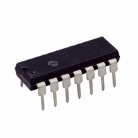
TC9402CPD Microchip Technology, TC9402CPD Datasheet - Page 7

TC9402CPD
Manufacturer Part Number
TC9402CPD
Description
IC V-FREQ/FREQ-V CONV 14DIP
Manufacturer
Microchip Technology
Type
Volt to Freq & Freq to Voltr
Specifications of TC9402CPD
Package / Case
14-DIP (0.300", 7.62mm)
Frequency - Max
100kHz
Full Scale
±100ppm/°C
Linearity
±0.25%
Mounting Type
Through Hole
Supply Voltage (max)
15 V
Supply Voltage (min)
8 V
Maximum Operating Temperature
70 C
Minimum Operating Temperature
0 C
Dual Supply Voltage
+/- 5 V
Full Scale Frequency
100 KHz
Linearity Error
+/- 0.5 % FSR
Maximum Dual Supply Voltage
+/- 7.5 V
Minimum Dual Supply Voltage
+/- 4 V
Mounting Style
Through Hole
Operating Supply Voltage
9 V or 12 V
Frequency
100kHz
Full Scale Range
1Hz To 100kHz
Linearity %
0.25%
Supply Voltage Range
± 4V To ± 7.5V
Digital Ic Case Style
DIP
No. Of Pins
14
Frequency Max
100kHz
Rohs Compliant
Yes
Lead Free Status / RoHS Status
Lead free / RoHS Compliant
Lead Free Status / RoHS Status
Lead free / RoHS Compliant, Lead free / RoHS Compliant
Other names
158-1142
158-1142
158-1142
3.0
3.1
The TC9400 V/F converter operates on the principal of
charge balancing. The operation of the TC9400 is eas-
ily understood by referring to Figure 3-1. The input volt-
age (V
resistor. This current is then converted to a charge on
the integrating capacitor and shows up as a linearly
decreasing voltage at the output of the op amp. The
lower limit of the output swing is set by the threshold
detector, which causes the reference voltage to be
applied to the reference capacitor for a time period long
enough to charge the capacitor to the reference volt-
age. This action reduces the charge on the integrating
capacitor by a fixed amount (q = C
the op amp output to step up a finite amount.
At the end of the charging period, C
This dissipates the charge stored on the reference
capacitor, so that when the output again crosses zero,
the system is ready to recycle. In this manner, the con-
tinued discharging of the integrating capacitor by the
input is balanced out by fixed charges from the refer-
FIGURE 3-1:
© 2006 Microchip Technology Inc.
IN
) is converted to a current (I
DETAILED DESCRIPTION
Voltage-to-Frequency (V/F) Circuit
Description
INPUT
0V –10V
V
IN
50 kΩ
820 pF
Adjust
Offset
C
R
INT
IN
1MΩ
+5V
-5V
10 Hz to 10 kHz V/F Converter
510 kΩ
C
180 pF
REF
11
12
10 kΩ
5
3
2
REF
I
REF
Zero Adjust
V
AMP OUT
IN
Threshold
Detect
-3V
REF
x V
IN
12 pF
is shorted out.
) by the input
OUT
REF
), causing
100 kΩ
R
BIAS
Start
Self-
Threshold
Detector
Op Amp
–
+
I
BIAS
20 kΩ
60 pF
1
ence voltage. As the input voltage is increased, the
number of reference pulses required to maintain
balance increases, which causes the output frequency
to also increase. Since each charge increment is fixed,
the increase in frequency with voltage is linear. In addi-
tion, the accuracy of the output pulse width does not
directly affect the linearity of the V/F. The pulse must
simply be long enough for full charge transfer to take
place.
The TC9400 contains a “self-start” circuit to ensure the
V/F converter always operates properly when power is
first applied. In the event that, during power-on, the op
amp output is below the threshold and C
charged, a positive voltage step will not occur. The op
amp output will continue to decrease until it crosses the
-3.0V threshold of the “self-start” comparator. When
this happens, an internal resistor is connected to the op
amp input, which forces the output to go positive until
the TC9400 is in its normal Operating mode.
The TC9400 utilizes low-power CMOS processing for
low input bias and offset currents, with very low power
dissipation. The open drain N-channel output FETs
provide high voltage and high current sink capability.
-5V
3μsec
Delay
4
V
+5V
V
SS
Reference Voltage
DD
14
(Typically -5V)
TC9400/9401/9402
V
7
REF
÷2
TC9400
TC9401
TC9402
GND
6
Common
Output
F
OUT
F
OUT
/2
8
10
9
DS21483C-page 7
+ 5V
+ 5V
REF
R
10 kΩ
R
10 kΩ
L
L
is already


