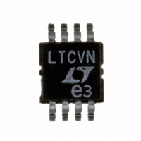
LTC6652BHMS8-4.096#PBF Linear Technology, LTC6652BHMS8-4.096#PBF Datasheet

LTC6652BHMS8-4.096#PBF
Specifications of LTC6652BHMS8-4.096#PBF
Available stocks
Related parts for LTC6652BHMS8-4.096#PBF
LTC6652BHMS8-4.096#PBF Summary of contents
Page 1
... The optional output capacitor can be left off when space constraints are critical. L, LT, LTC, LTM, Linear Technology and the Linear logo are registered trademarks of Linear Technology Corporation. All other trademarks are the property of their respective owners. 0.050 ...
Page 2
... LTC6652BHMS8-3#TRPBF LTC6652AHMS8-3.3#PBF LTC6652AHMS8-3.3#TRPBF LTC6652BHMS8-3.3#PBF LTC6652BHMS8-3.3#TRPBF LTC6652AHMS8-4.096#PBF LTC6652AHMS8-4.096#TRPBF LTC6652BHMS8-4.096#PBF LTC6652BHMS8-4.096#TRPBF LTC6652AHMS8-5#PBF LTC6652AHMS8-5#TRPBF LTC6652BHMS8-5#PBF LTC6652BHMS8-5#TRPBF Consult LTC Marketing for parts specifi ed with wider operating temperature ranges. *The temperature grade is identifi label on the shipping container. Consult LTC Marketing for information on non-standard lead based fi nish parts. ...
Page 3
ELECTRICAL CHARACTERISTICS temperature range, otherwise specifi cations are at T PARAMETER CONDITIONS Output Voltage LTC6652A LTC6652B Output Voltage Temperature Coeffi cient LTC6652A (Note 3) LTC6652B Line Regulation V Load Regulation (Note 4) I SOURCE LTC6652-2.5, LTC6652-3, LTC6652-3.3, LTC6652-4.096, LTC6652-5 I ...
Page 4
LTC6652 TYPICAL PERFORMANCE CHARACTERISTICS LTC6652s. Curves from the LTC6652-1.25, LTC6652-2.5 and the LTC6652-5 represent the extremes and typical of the voltage options. Characteristic curves for other output voltages fall between these curves and can be estimated based on their output. ...
Page 5
TYPICAL PERFORMANCE CHARACTERISTICS LTC6652s. Curves from the LTC6652-1.25, LTC6652-2.5 and the LTC6652-5 represent the extremes and typical of the voltage options. Characteristic curves for other output voltages fall between these curves and can be estimated based on their output. 2.5V ...
Page 6
LTC6652 TYPICAL PERFORMANCE CHARACTERISTICS LTC6652s. Curves from the LTC6652-1.25, LTC6652-2.5 and the LTC6652-5 represent the extremes and typical of the voltage options. Characteristic curves for other output voltages fall between these curves and can be estimated based on their output. ...
Page 7
TYPICAL PERFORMANCE CHARACTERISTICS LTC6652s. Curves from the LTC6652-1.25, LTC6652-2.5 and the LTC6652-5 represent the extremes and typical of the voltage options. Characteristic curves for other output voltages fall between these curves and can be estimated based on their output. 5V ...
Page 8
LTC6652 TYPICAL PERFORMANCE CHARACTERISTICS LTC6652s. Curves from the LTC6652-1.25, LTC6652-2.5 and the LTC6652-5 represent the extremes and typical of the voltage options. Characteristic curves for other output voltages fall between these curves and can be estimated based on their output. ...
Page 9
BLOCK DIAGRAM SHDN 3 GND 4 APPLICATIONS INFORMATION Bypass and Load Capacitors The LTC6652 voltage references do not require an input capacitor, but a 0.1μF capacitor located close to the part improves power supply rejection. The LTC6652 ...
Page 10
LTC6652 APPLICATIONS INFORMATION 3. OUT 500mV/DIV C = 0μF 500μs/DIV OUT Figure 2. Transient Response Without Output Capacitor 3. OUT 500mV/DIV C = 1μF 500μs/DIV OUT Figure 3. Transient Response with 1μF ...
Page 11
APPLICATIONS INFORMATION V IN 2V/DIV V OUT 1V/DIV C = 0μF 100μs/DIV OUT Figure 8. Start-Up Response Without Output Capacitor V IN 2V/DIV V OUT 1V/DIV C = 1μF 100μs/DIV OUT Figure 9. Start-Up Response with 1μF Output Capacitor In ...
Page 12
LTC6652 APPLICATIONS INFORMATION 80 LTC6652-2.5 MS8 PACKAGE 3 TYPICAL PARTS –20 –40 0 300 600 900 HOURS Figure 12. Long-Term Drift Hysteresis The hysteresis data shown in Figure 13 represents the ...
Page 13
APPLICATIONS INFORMATION When operated within its specifi ed limits of V and sourcing 5mA, the LTC6652-2.5 consumes just under 60mW at room temperature. At 125°C the quiescent cur- rent will be slightly higher and the power consumption 300 380s T ...
Page 14
LTC6652 TYPICAL APPLICATIONS Extended Supply Range Reference 4V TO 30V R1 V LTC6652-2 SHDN BZX84C18 GND C1 6652 TA02 0.1μF Negative Rail Circuit V ≥ 1.75V 0.1μF 6 LTC6652-2 500Ω ...
Page 15
... Change to Typical Performance Characteristics Change to Typical Application Information furnished by Linear Technology Corporation is believed to be accurate and reliable. However, no responsibility is assumed for its use. Linear Technology Corporation makes no representa- tion that the interconnection of its circuits as described herein will not infringe on existing patent rights. LTC6652 ...
Page 16
... Max, 10ppm/°C Max, 60μA Supply, SOT23 Package 0.5% Max, 5.6μA Supply, SOT23 Package 0.2% Max, 20ppm/°C Max, 20mA Output Current, 2mm × 2mm DFN www.linear.com ● VDAC REF LTC1605 16 A/D D OUT GND 6652 TA05 6652fc LT 1109 REV C • PRINTED IN USA © LINEAR TECHNOLOGY CORPORATION 2007 ...


