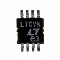
LTC6652BHMS8-4.096#PBF Linear Technology, LTC6652BHMS8-4.096#PBF Datasheet - Page 8

LTC6652BHMS8-4.096#PBF
Manufacturer Part Number
LTC6652BHMS8-4.096#PBF
Description
IC REF PREC LN 8-MSOP
Manufacturer
Linear Technology
Datasheet
1.LTC6652BHMS8-4.096PBF.pdf
(16 pages)
Specifications of LTC6652BHMS8-4.096#PBF
Reference Type
Series
Voltage - Output
4.096V
Tolerance
±0.1%
Temperature Coefficient
10ppm/°C
Voltage - Input
4.596 ~ 13.2 V
Number Of Channels
1
Current - Quiescent
350µA
Current - Output
16mA
Operating Temperature
-40°C ~ 125°C
Mounting Type
Surface Mount
Package / Case
8-MSOP, Micro8™, 8-uMAX, 8-uSOP,
Fixed / Adjust / Prog
Precision
Output Voltage (max)
4.096V
Reference Voltage Accuracy (max)
0.1
Line Regulation
50ppm/V
Load Regulation
150ppm/mA
Input Voltage (max)
13.2V
Operating Temp Range
-40C to 125C
Operating Temperature Classification
Automotive
Mounting
Surface Mount
Pin Count
8
Package Type
MSOP
Lead Free Status / RoHS Status
Lead free / RoHS Compliant
Current - Cathode
-
Lead Free Status / Rohs Status
Compliant
Available stocks
Company
Part Number
Manufacturer
Quantity
Price
LTC6652
PIN FUNCTIONS
DNC (Pin 1): Do Not Connect.
V
V
supply is 13.2V. Bypassing V
GND will improve PSRR.
SHDN (Pin 3): Shutdown Input. This active low input
powers down the device to <2μA. For normal operation
tie this pin to V
LTC6652s. Curves from the LTC6652-1.25, LTC6652-2.5 and the LTC6652-5 represent the extremes and typical of the voltage options.
Characteristic curves for other output voltages fall between these curves and can be estimated based on their output.
8
TYPICAL PERFORMANCE CHARACTERISTICS
IN
OUT
–100
–10
–20
–30
–40
–50
–60
–70
–80
–90
(Pin 2): Power Supply. The minimum supply input is
0
0.01
+ 300mV or 2.7V; whichever is higher. The maximum
Power Supply Rejection Ratio
vs Frequency
0.1
FREQUENCY (kHz)
IN
.
1
C
OUT
10
C
= 0μF
OUT
C
OUT
= 10μF
100
IN
= 1μF
with a 0.1μF capacitor to
6652 G07
1000
100
0.1
10
1
0.01
Output Impedance vs Frequency
0.1
FREQUENCY (kHz)
C
OUT
C
OUT
= 1μF
1
GND (Pin 4): Device Ground.
V
required. For some applications, a capacitor between 0.1μF
to 10μF can be benefi cial. See the graphs in the Typical
Performance Characteristics section for further details.
GND (Pins 5,7,8): Internal Function. Ground these pins.
OUT
= 10μF
C
OUT
= 0μF
(Pin 6): Output Voltage. An output capacitor is not
10
Characteristic curves are similar for most
6652 G08
100
2.5
2.0
1.0
1.5
0.5
0
2
SHDN Input Voltage Thresholds
vs V
IN
4
6
V
IN
8
(V)
V
10
TH(UP)
V
TH(DN)
12
6652 G13
6652fc
14


