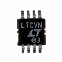
LTC6652BHMS8-4.096#PBF Linear Technology, LTC6652BHMS8-4.096#PBF Datasheet - Page 11

LTC6652BHMS8-4.096#PBF
Manufacturer Part Number
LTC6652BHMS8-4.096#PBF
Description
IC REF PREC LN 8-MSOP
Manufacturer
Linear Technology
Datasheet
1.LTC6652BHMS8-4.096PBF.pdf
(16 pages)
Specifications of LTC6652BHMS8-4.096#PBF
Reference Type
Series
Voltage - Output
4.096V
Tolerance
±0.1%
Temperature Coefficient
10ppm/°C
Voltage - Input
4.596 ~ 13.2 V
Number Of Channels
1
Current - Quiescent
350µA
Current - Output
16mA
Operating Temperature
-40°C ~ 125°C
Mounting Type
Surface Mount
Package / Case
8-MSOP, Micro8™, 8-uMAX, 8-uSOP,
Fixed / Adjust / Prog
Precision
Output Voltage (max)
4.096V
Reference Voltage Accuracy (max)
0.1
Line Regulation
50ppm/V
Load Regulation
150ppm/mA
Input Voltage (max)
13.2V
Operating Temp Range
-40C to 125C
Operating Temperature Classification
Automotive
Mounting
Surface Mount
Pin Count
8
Package Type
MSOP
Lead Free Status / RoHS Status
Lead free / RoHS Compliant
Current - Cathode
-
Lead Free Status / Rohs Status
Compliant
Available stocks
Company
Part Number
Manufacturer
Quantity
Price
In Figure 8, ripple momentarily appears just after the
leading edge of powering on. This brief one time event is
caused by calibration circuitry during initialization. When
an output capacitor is used, the ripple is virtually undetect-
able as shown in Figure 9.
Shutdown Mode
Shutdown mode is enabled by tying SHDN low which places
the part in a low power state (i.e., <2μA). In shutdown
mode, the output pin takes the value 20k • (rated output
voltage). For example, an LTC6652-2.5 will have an output
impedance of 20k • 2.5 = 50kΩ. For normal operation,
SHDN should be greater than or equal to 2.0V. For use
with a microcontroller, use a pull-up resistor to V
an open-drain output driver as shown in Figure 10. The
LTC6652’s response into and out of shutdown mode is
shown in Figure 11.
APPLICATIONS INFORMATION
Figure 9. Start-Up Response with 1μF Output Capacitor
Figure 8. Start-Up Response Without Output Capacitor
2V/DIV
1V/DIV
2V/DIV
1V/DIV
V
V
OUT
OUT
V
V
IN
IN
C
C
OUT
OUT
= 0μF
= 1μF
100μs/DIV
100μs/DIV
6652 F08
6652 F09
IN
and
The trip thresholds on SHDN have some dependence
on the voltage applied to V
Performance Characteristics section. Be careful to avoid
leaving SHDN at a voltage between the thresholds as
this will likely cause an increase in supply current due to
shoot-through current.
Long-Term Drift
Long-term drift cannot be extrapolated from acceler-
ated high temperature testing. This erroneous technique
gives drift numbers that are wildly optimistic. The only
way long-term drift can be determined is to measure it
over the time interval of interest. The LTC6652 long-term
drift data was collected on more than 100 parts that were
soldered into PC boards similar to a “real world” application.
The boards were then placed into a constant temperature
oven with T
and measured with an 8.5 digit DVM. Long-term drift is
shown below in Figure 12.
2.8V V
1V/DIV
1V/DIV
SHDN
V
OUT
Figure 11. Shutdown Response with 5mA Load
IN
Figure 10. Open-Drain Shutdown Circuit
I
13.2V
A
LOAD
= 35°C, their outputs were scanned regularly
TO μC
= 5mA
C1
1μF
2N7002
R1
20k
1ms/DIV
SHDN
IN
LTC6652-2.5
as shown in the Typical
GND
V
IN
LTC6652
V
6652 F10
OUT
6652 F11
C2
1μF
11
V
OUT
6652fc


