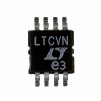
LTC6652BHMS8-4.096#PBF Linear Technology, LTC6652BHMS8-4.096#PBF Datasheet - Page 9

LTC6652BHMS8-4.096#PBF
Manufacturer Part Number
LTC6652BHMS8-4.096#PBF
Description
IC REF PREC LN 8-MSOP
Manufacturer
Linear Technology
Datasheet
1.LTC6652BHMS8-4.096PBF.pdf
(16 pages)
Specifications of LTC6652BHMS8-4.096#PBF
Reference Type
Series
Voltage - Output
4.096V
Tolerance
±0.1%
Temperature Coefficient
10ppm/°C
Voltage - Input
4.596 ~ 13.2 V
Number Of Channels
1
Current - Quiescent
350µA
Current - Output
16mA
Operating Temperature
-40°C ~ 125°C
Mounting Type
Surface Mount
Package / Case
8-MSOP, Micro8™, 8-uMAX, 8-uSOP,
Fixed / Adjust / Prog
Precision
Output Voltage (max)
4.096V
Reference Voltage Accuracy (max)
0.1
Line Regulation
50ppm/V
Load Regulation
150ppm/mA
Input Voltage (max)
13.2V
Operating Temp Range
-40C to 125C
Operating Temperature Classification
Automotive
Mounting
Surface Mount
Pin Count
8
Package Type
MSOP
Lead Free Status / RoHS Status
Lead free / RoHS Compliant
Current - Cathode
-
Lead Free Status / Rohs Status
Compliant
Available stocks
Company
Part Number
Manufacturer
Quantity
Price
BLOCK DIAGRAM
APPLICATIONS INFORMATION
Bypass and Load Capacitors
The LTC6652 voltage references do not require an input
capacitor, but a 0.1μF capacitor located close to the part
improves power supply rejection.
The LTC6652 voltage references are stable with or without
a capacitive load. For applications where an output capaci-
tor is benefi cial, a value of 0.1μF to 10μF is recommended
depending on load conditions. The Typical Performance
Characteristics section includes a plot illustrating a region
of marginal stability. Either no or low value capacitors for
any load current are acceptable. For loads that sink current
or light loads that source current, a 0.1μF to 10μF capacitor
has stable operation. For heavier loads that source current
a 0.5μF to 10μF capacitor range is recommended.
2
3
4
V
SHDN
GND
IN
V
0.1μF
3V
IN
C
IN
2, 3
Figure 1. Transient Load Test Circuit
LTC6652-2.5
4, 5, 7, 8
BANDGAP
6
The transient response for a 0.5V step on V
without an output capacitor is shown in Figures 2 and 3,
respectively.
The LTC6652 references with an output of 2.5V and above
are guaranteed to source and sink 5mA. The 1.25V and
2.048V versions are guaranteed to source 5mA and sink
1mA. The test circuit for transient load step response is
shown in Figure 1. Figures 4 and 5 show a 5mA source
and sink load step response without a load capacitor,
respectively.
Start-Up
The start-up characteristic of the LTC6652 is shown in
Figures 8 and 9. Note that the turn-on time is affected by
the value of the output capacitor.
100Ω
C
1μF
OUT
–
+
6652 F01
V
GEN
0.5V
6652 BD
V
OUT
6
LTC6652
IN
with and
6652fc
9


