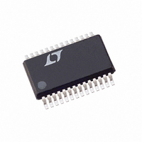
LTC1873EG#TR Linear Technology, LTC1873EG#TR Datasheet - Page 11

LTC1873EG#TR
Manufacturer Part Number
LTC1873EG#TR
Description
IC REG SW 2PH DUAL SYNC 28SSOP
Manufacturer
Linear Technology
Datasheet
1.LTC1873EG.pdf
(32 pages)
Specifications of LTC1873EG#TR
Pwm Type
Voltage Mode
Number Of Outputs
2
Frequency - Max
750kHz
Duty Cycle
93%
Voltage - Supply
3 V ~ 7 V
Buck
Yes
Boost
No
Flyback
No
Inverting
No
Doubler
No
Divider
No
Cuk
No
Isolated
No
Operating Temperature
-40°C ~ 85°C
Package / Case
28-SSOP
Frequency-max
750kHz
Lead Free Status / RoHS Status
Contains lead / RoHS non-compliant
Available stocks
Company
Part Number
Manufacturer
Quantity
Price
APPLICATIO S I FOR ATIO
pin. The output is connected to COMP, which is in turn
connected to the soft-start circuitry and from there to the
PWM generator.
Unlike many regulators that use a resistor divider con-
nected to a high impedance feedback input, the LTC1873
is designed to use an inverting summing amplifier topol-
ogy with the FB pin configured as a virtual ground. This
allows flexibility in choosing pole and zero locations not
available with simple g
allows the use of “type 3” compensation, which provides
a phase boost at the LC pole frequency and significantly
improves loop phase margin (see Figure 3). The Feedback
Loop/Compensation section contains a detailed explana-
tion of type 3 feedback loops. Note that side 1 of the
LTC1873 includes R1 and R
DAC circuitry.
MIN/MAX COMPARATORS
Two additional feedback loops keep an eye on the primary
feedback amplifier and step in if the feedback node moves
(see Block Diagram) activates whenever FB rises more
than 5% above 800mV. It immediately turns the top
MOSFET (QT) off and the bottom MOSFET (QB) on and
keeps them that way until FB falls back within 5% of its
nominal value. This pulls the output down as fast as
possible, preventing damage to the (often expensive)
load. If FB rises because the output is shorted to a higher
supply, QB will stay on until the short goes away, the
higher supply current limits or QB dies trying to save the
load. This behavior provides maximum protection against
overvoltage faults at the output, while allowing the circuit
5% from its nominal 800mV value. The MAX comparator
COMP
Figure 3. “Type 3” Feedback Loop (Side 2 Shown)
R2
FB
C2
U
+
–
m
U
configurations. In particular, it
0.8V
C1
B
FB
internally as part of the VID
W
1873 F03
R
B
R3
R1
C3
U
V
OUT
to resume normal operation when the fault is removed.
The overvoltage protection circuit can optionally be set to
latch the output off permanently (see the Overvoltage Fault
section).
The MIN comparator (see Block Diagram) trips whenever
FB is more than 5% below 800mV and immediately forces
the switch duty cycle to 90% to bring the output voltage
back into range. It releases when FB is within the 5%
window. MIN is disabled when the soft-start or current
limit circuits are active—the only two times that the
output should legitimately be below its regulated value.
Notice that the FB pin is the virtual ground node of the
feedback amplifier. A typical compensation network does
not include local DC feedback around the amplifier, so that
the DC level at FB will be an accurate replica of the output
voltage, divided down by R1 and R
the compensation capacitors will tend to attenuate AC
signals at FB, especially with low bandwidth type 1 feed-
back loops. This creates a situation where the MIN and
MAX comparators do not respond immediately to shifts in
the output voltage, since they monitor the output at FB.
Maximizing feedback loop bandwidth will minimize these
delays and allow MIN and MAX to operate properly. See
the Feedback Loop/Compensation section.
SHUTDOWN/SOFT-START
Each half of the LTC1873 has a RUN/SS pin. The RUN/SS
pins perform two functions: when pulled to ground, each
shuts down its half of the LTC1873, and each acts as a
conventional soft-start pin, enforcing a maximum duty
cycle limit proportional to the voltage at RUN/SS. An
internal 3.5 A current source pull-up is connected to each
RUN/SS pin, allowing a soft-start ramp to be generated
with a single external capacitor to ground. The 3.5 A
current sources are active even when the LTC1873 is shut
down, ensuring the device will start when any external
pull-down at RUN/SS is released. Either side can be shut
down without affecting the operation of the other side. If
both sides are shut down at the same time, the LTC1873
goes into a micropower sleep mode, and quiescent cur-
rent drops typically below 50 A. Entering sleep mode also
resets the FAULT latch, if it was set.
B
(Figure 3). However,
LTC1873
11


