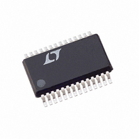
LTC1873EG#TR Linear Technology, LTC1873EG#TR Datasheet - Page 3

LTC1873EG#TR
Manufacturer Part Number
LTC1873EG#TR
Description
IC REG SW 2PH DUAL SYNC 28SSOP
Manufacturer
Linear Technology
Datasheet
1.LTC1873EG.pdf
(32 pages)
Specifications of LTC1873EG#TR
Pwm Type
Voltage Mode
Number Of Outputs
2
Frequency - Max
750kHz
Duty Cycle
93%
Voltage - Supply
3 V ~ 7 V
Buck
Yes
Boost
No
Flyback
No
Inverting
No
Doubler
No
Divider
No
Cuk
No
Isolated
No
Operating Temperature
-40°C ~ 85°C
Package / Case
28-SSOP
Frequency-max
750kHz
Lead Free Status / RoHS Status
Contains lead / RoHS non-compliant
Available stocks
Company
Part Number
Manufacturer
Quantity
Price
ELECTRICAL CHARACTERISTICS
The
V
SYMBOL
Switching Characteristics
V
f
DC
DC
DC
t
t
Feedback Amplifier
A
GBW
I
V
V
Current Limit Loop
A
I
Status Outputs
V
V
I
t
VID Inputs
R1
V
R
VID
I
V
Note 1: Absolute Maximum Ratings are those values beyond which the life
of a device may be impaired.
Note 2: The LTC1873 is guaranteed to meet performance specifications
from 0 C to 70 C. Specifications over the – 40 C to 85 C operating
temperature range are assured by design, characterization and correlation
with statistical process controls.
Note 3: PV
the external MOSFETs used to ensure proper operation.
Note 4: All currents into device pins are positive; all currents out of device
pins are negative. All voltages are referenced to ground unless otherwise
specified.
OSC
NOV
ERR
IMAX
FAULT
FAULT
VID-LEAK
r
OSC
, t
VFB
MIN
MAX
VILIM
FAULT
OLF
OUT
PULLUP
CC
PULLUP
OSC2
MIN1
MIN2
MAX
f
T
= 5V unless otherwise specified. (Note 4)
Error % Output Voltage Accuracy
denotes specifications which apply over the full operating temperature range, otherwise specifications are T A = 25 C.
CC
and BV
PARAMETER
Oscillator Amplitude
Oscillator Frequency
Controller 2 Oscillator Phase
Minimum Duty Cycle
Minimum Duty Cycle
Maximum Duty Cycle
Driver Nonoverlap
Driver Rise/Fall Time
FB DC Gain
FB Gain Bandwidth
FB Sink/Source Current
MIN Comparator Threshold
MAX Comparator Threshold
I
I
FAULT Trip Point
FAULT Output Low Voltage
FAULT Output Current
FAULT Delay Time
Resistance Between SENSE and FB1
VID Input Pull-Up Resistance
VID Input Voltage Threshold
VID Input Leakage Current
VID Pull-Up Voltage
LIM
MAX
Gain
CC
Source Current
(V
BOOST
– V
SW
) must be greater than V
GS(ON)
Test Circuit 1 (Note 9)
CONDITIONS
Test Circuit 1
Relative to Controller 1
V
V
Test Circuit 1 (Note 9)
COMP
I
V
I
V
V
Side 1 Only
Programmed from 1.3V to 3.5V
V
V
V
V
V
V
MAX
FAULT
FB
FB
FB
FAULT
FB
DIODE
IL
IH
CC
CC
CC
(2.7V V
(2.7V V
< V
> V
Relative to Regulated V
> V
< VID < 7V (Note 8)
= 3.3V
= 5V
= 0V
of
N
= 1mA
= 0V
= 0.6V (Note 8)
MAX
MAX
FAULT
Output
CC
to FAULT
CC
Note 5: Supply current in normal operation is dominated by the current
needed to charge and discharge the external MOSFET gates. This current
will vary with supply voltage and the external MOSFETs used.
Note 6: Supply current in shutdown is dominated by external MOSFET
leakage and may be significantly higher than the quiescent current drawn
by the LTC1873, especially at elevated temperature.
Note 7: Feedback current at FB1 will be higher due to internal VID
resistors.
Note 8: Each built-in pull-up resistor attached to the VID inputs also has a
series diode connected to V
supply without damage or clamping. (See Block Diagram.)
Note 9: Rise and fall times are measured at 20% to 80% levels. Delay and
nonoverlap times are measured using 50% levels.
5.5V)
5.5V)
(Note 9)
OUT
CC
to allow input voltages higher than the V
– 1.5
MIN
+ 10
475
815
1.6
– 7
87
74
7
0
3
0.03
0.01
TYP
550
180
760
840
–10
+ 15
– 10
2.8
4.5
10
90
40
12
85
25
40
25
20
40
1
10
LTC1873
MAX
–14
+ 20
750
100
785
0.1
1.5
0.4
93
80
1
UNITS
3
DEG
MHz
V
CC
kHz
mA
mV
mV
P-P
k
k
dB
dB
ns
ns
%
%
%
%
%
A
V
A
V
V
A
V
V
s


