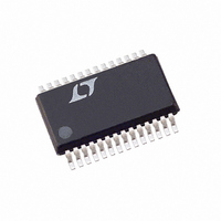
LTC1873EG#TR Linear Technology, LTC1873EG#TR Datasheet - Page 9

LTC1873EG#TR
Manufacturer Part Number
LTC1873EG#TR
Description
IC REG SW 2PH DUAL SYNC 28SSOP
Manufacturer
Linear Technology
Datasheet
1.LTC1873EG.pdf
(32 pages)
Specifications of LTC1873EG#TR
Pwm Type
Voltage Mode
Number Of Outputs
2
Frequency - Max
750kHz
Duty Cycle
93%
Voltage - Supply
3 V ~ 7 V
Buck
Yes
Boost
No
Flyback
No
Inverting
No
Doubler
No
Divider
No
Cuk
No
Isolated
No
Operating Temperature
-40°C ~ 85°C
Package / Case
28-SSOP
Frequency-max
750kHz
Lead Free Status / RoHS Status
Contains lead / RoHS non-compliant
Available stocks
Company
Part Number
Manufacturer
Quantity
Price
APPLICATIO S I FOR ATIO
factor of 3.75. The reduced input ripple voltage also means
less power is lost in the input power path, which could
include batteries, switches, trace/connector resistances
and protection circuitry. Improvements in both conducted
and radiated EMI also directly accrue as a result of the
reduced RMS input current and voltage.
Small Footprint
The LTC1873 operates at a 550kHz switching frequency,
allowing it to use low value inductors without generating
excessive ripple currents. Because the inductor stores
less energy per cycle, the physical size of the inductor can
be reduced without risking core saturation, saving PCB
board space. The high operating frequency also means
less energy is stored in the output capacitors between
cycles, minimizing their required value and size. The
remaining components, including the SSOP-28 LTC1873,
are tiny, allowing an entire dual-output LTC1873 circuit to
be constructed in 1.5in
is generally located right next to the microprocessor or in
some similarly congested area, where PCB real estate is at
a premium.
Fast Transient Response
The LTC1873 uses a fast 25MHz GBW op amp as an error
amplifier. This allows the compensation network to be
designed with several poles and zeros in a more flexible
configuration than with a typical g
The high bandwidth of the amplifier, coupled with the high
switching frequency and the low values of the external
inductor and output capacitor, allow very high loop cross-
over frequencies. The low inductor value is the other half
of the equation—with a typical value on the order of 1 H,
the inductor allows very fast di/dt slew rates. The result is
superior transient response compared with conventional
solutions.
High Efficiency
The LTC1873 uses a synchronous step-down (buck)
architecture, with two external N-channel MOSFETs per
output. A floating topside driver and a simple external
charge pump provide full gate drive to the upper MOSFET.
U
2
of PCB space. Further, this space
U
W
m
feedback amplifier.
U
The voltage mode feedback loop and MOSFET V
limit sensing remove the need for an external current
sense resistor, eliminating an external component and a
source of power loss in the high current path. Properly
designed circuits using low gate charge MOSFETs are
capable of efficiencies exceeding 90% over a wide range
of output voltages.
VID Programming
The LTC1873 includes an onboard feedback network that
programs the output voltage at side 1 in accordance with
the Intel Desktop VID specification (Table 1). The network
includes a 20k resistor (R1) connected from SENSE to
FB1, and a variable value resistor (R
with the value set by the digital code present at the VID0:4
pins. SENSE should be connected to V
network to monitor the output voltage. No additional
feedback components are required to set the output volt-
age at controller 1, although loop compensation compo-
nents are still required. Each VID n pin includes an internal
40k pull-up resistor, allowing it to float high if left uncon-
nected. The pull-up resistors are connected to V
diodes (see Block Diagram), allowing the VID n pins to be
pulled above V
Note that code 11111, defined by Intel to indicate “no CPU
present,” does generate an output voltage at V
Note also that controller 2 on the LTC1873 is not con-
nected to the VID circuitry, and works independently from
controller 1.
ARCHITECTURE DETAILS
The LTC1873 dual switching regulator controller includes
two independent regulator channels. The two sides of the
chip and their corresponding external components act
independently of each other with the exception of the
common input bypass capacitor, the VID circuitry at side
1, and the FCB and FAULT pins, which affect both chan-
nels. In the following discussions, when a pin is referred
to without mentioning which side is involved, that discus-
sion applies equally to both sides.
CC
without damage.
B
) from FB1 to SGND,
OUT1
LTC1873
OUT1
to allow the
CC
DS
(2.00V).
through
current
9


