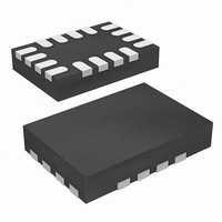
ISL62871HRUZ-T Intersil, ISL62871HRUZ-T Datasheet - Page 19

ISL62871HRUZ-T
Manufacturer Part Number
ISL62871HRUZ-T
Description
IC CTRLR DC/DC PWM 16-TQFN
Manufacturer
Intersil
Datasheet
1.ISL62871HRUZ-T.pdf
(25 pages)
Specifications of ISL62871HRUZ-T
Pwm Type
Controller
Number Of Outputs
1
Frequency - Max
330kHz
Duty Cycle
100%
Voltage - Supply
3.3 V ~ 25 V
Buck
Yes
Boost
No
Flyback
No
Inverting
No
Doubler
No
Divider
No
Cuk
No
Isolated
No
Operating Temperature
-10°C ~ 100°C
Package / Case
16-UTQFN (16-µTQFN)
Frequency-max
330kHz
Lead Free Status / RoHS Status
Lead free / RoHS Compliant
Available stocks
Company
Part Number
Manufacturer
Quantity
Price
Part Number:
ISL62871HRUZ-T
Manufacturer:
INTERSIL
Quantity:
20 000
.
Driver Power Dissipation
Switching power dissipation in the driver is mainly a function
of the switching frequency and total gate charge of the
selected MOSFETs. Calculating the power dissipation in the
driver for a desired application is critical to ensuring safe
operation. Exceeding the maximum allowable power
dissipation level will push the IC beyond the maximum
recommended operating junction temperature of +125°C.
When designing the application, it is recommended that the
following calculation be performed to ensure safe operation
at the desired frequency for the selected MOSFETs. The
power dissipated by the drivers is approximated as
Equation 38:
Where:
P
FIGURE 15. BOOT CAPACITANCE vs BOOT RIPPLE VOLTAGE
- F
- V
- V
- Q
- Q
- P
- P
=
the gate of the MOSFET and discrete capacitors
the gate of the MOSFET and discrete capacitors
driver
driver
F
sw
sw
U
L
L
U
2.0
1.8
1.6
1.4
1.2
1.0
0.8
0.6
0.4
0.2
0.0
U
L
is the lower gate driver bias supply voltage
is the quiescent power consumption of the lower
is the charge to be delivered by the lower driver into
is the upper gate driver bias supply voltage
is the quiescent power consumption of the upper
0.0
is the charge to be delivered by the upper driver into
(
is the switching frequency of the PWM signal
1.5V
20nC
0.1
U
Q
U
0.2
+
Q
GATE
V
L
Q
0.3
L
= 100nC
)
DV
+
0.4
P
19
BOOT_CAP
L
+
0.5
P
U
0.6
(V)
0.7
0.8
ISL62871, ISL62872
0.9
(EQ. 38)
1.0
P
MOSFET Selection and Considerations
Typically, a MOSFET cannot tolerate even brief excursions
beyond their maximum drain to source voltage rating. The
MOSFETs used in the power stage of the converter should
have a maximum V
upper voltage tolerance of the input power source and the
voltage spike that occurs when the MOSFET switches off.
There are several power MOSFETs readily available that are
optimized for DC/DC converter applications. The preferred
high-side MOSFET emphasizes low switch charge so that
the device spends the least amount of time dissipating
power in the linear region. Unlike the low-side MOSFET
which has the drain-source voltage clamped by its body
diode during turn-off, the high-side MOSFET turns off with
V
MOSFET emphasizes low r
minimize conduction loss.
For the low-side MOSFET, (LS), the power loss can be
assumed to be conductive only and is written as
Equation 39:
For the high-side MOSFET, (HS), its conduction loss is
written as Equation 40:
For the high-side MOSFET, its switching loss is written as
Equation 41:
P
P
SW_HS
IN
CON_LS
CON_HS
1000
- V
900
800
700
600
500
400
300
200
100
FIGURE 16. POWER DISSIPATION vs FREQUENCY
OUT
0
0
=
≈
, plus the spike, across it. The preferred low-side
=
V
--------------------------------------------------------------------- -
I
Q
Q
200
LOAD
IN
I
U
L
LOAD
=200nC
=100nC
⋅
I
VALLEY
400
2
2
r ⋅
DS
r ⋅
DS ON
600
DS ON
2
rating that exceeds the sum of the
(
Q
(
⋅
Q
L
t
FREQUENCY (Hz)
ON
U
=100nC
800 1k
)_LS
=50nC
DS(ON)
)_HS
⋅
F
⋅
SW
(
⋅
1 D
D
–
+
when fully saturated to
1.2k 1.4k 1.6k 1.8k 2k
V
----------------------------------------------------------------- -
)
IN
⋅
I
PEAK
Q
Q
2
⋅
U
L
Q
Q
August 14, 2008
t
=50nC
=50nC
OFF
U
L
=50nC
=20nC
(EQ. 39)
(EQ. 40)
(EQ. 41)
FN6707.0
⋅
F
SW


