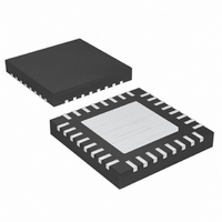
MAX17528GTJ+ Maxim Integrated Products, MAX17528GTJ+ Datasheet - Page 16

MAX17528GTJ+
Manufacturer Part Number
MAX17528GTJ+
Description
IC PWM CTRLR STP-DWN 32TQFN-EP
Manufacturer
Maxim Integrated Products
Series
Quick-PWM™r
Datasheet
1.MAX17528GTJ.pdf
(41 pages)
Specifications of MAX17528GTJ+
Applications
Controller, Intel IMVP-6.5™ GMCH
Voltage - Input
4.5 ~ 5.5 V
Number Of Outputs
1
Voltage - Output
0.01 ~ 1.5 V
Operating Temperature
-40°C ~ 105°C
Mounting Type
Surface Mount
Package / Case
32-TQFN Exposed Pad
Lead Free Status / RoHS Status
Lead free / RoHS Compliant
1-Phase Quick-PWM
Intel IMVP-6.5/GMCH Controllers
16
14–20
PIN
______________________________________________________________________________________
12
13
21
22
23
24
25
26
27
CLKEN
D0–D6
PGDIN
NAME
PGND
GND
V
BST
DH
DL
LX
DD
Dual-Function GMCH/IMVP-6.5 Select Input and Active-Low IMVP-6.5 CPU Clock Enable Open-
Drain Output. Connect to system 3.3V supply through pullup resistors for proper IMVP-6.5
operation. CLKEN voltage has to be higher than 2.3V before SHDN is pulled high. Connect to GND
to select the Intel GMCH feature set. This active-low logic output indicates when the feedback
voltage is in regulation. The MAX17528 forces CLKEN low during dynamic VID transitions and for
an additional 20µs after the VID transition is completed. CLKEN is the inverse of PWRGD, except
for the 5ms PWRGD startup delay period after CLKEN is pulled low. See the startup timing diagram
(Figure 9). The CLKEN upper threshold is blanked during any downward output-voltage transition
that happens when the MAX17528 are in skip mode, and stays blanked until the transition-related
PWRGD blanking period is complete and the output reaches regulation.
Analog Ground
Low-Voltage (1.0V Logic) VID DAC Code Inputs. The D0–D6 inputs do not have internal pullups.
These 1.0V logic inputs are designed to interface directly with the CPU. The output voltage is set
by the VID code indicated by the logic-level voltages on D0–D6 (see Table 2).
The 1111111 code corresponds to standby mode. When this code is detected, the MAX17528
enters standby mode while in forced-PWM mode, and slews to 0V at 1/8 the slew rate set by the
TIME resistor. After slewing to 0V, the IC enters skip mode (DH and DL low). If D6–D0 is changed
from 1111111 to a different code, the MAX17528 exits standby mode (while in skip mode) and
slews the output voltage to the target voltage set by the VID code at 1x the slew rate set by the
TIME resistor. Note that the standby supply current consumed by the MAX17528 is the same as its
quiescent supply current, because no analog blocks are turned off. This is necessary because of
the fast wake-up requirement.
Power Ground. Ground connection for the DL driver. Also used as an input to the MAX17528’s zero-
crossing comparator.
Low-Side Gate-Driver Output. DL swings from PGND to V
forced low in skip mode after detecting an inductor current zero-crossing.
Supply Voltage Input for the DL Driver. V
the BST flying capacitor during the time DL is high. Connect V
voltage. Bypass V
Boost Flying Capacitor Connection. BST provides the upper supply rail for the DH high-side gate
driver. An internal switch between V
MOSFET is on (DL pulled high and LX pulled to ground).
Inductor Connection. LX is the internal lower supply rail for the DH high-side gate driver. Also used
as an input to the MAX17528’s zero-crossing comparator.
High-Side Gate-Driver Output. DH swings from LX to BST. The controller pulls DH low in shutdown.
IMVP-6.5 Power-Good Logic Input. PGDIN indicates the power status of other system rails used to
power the chipset and CPU V
MAX17528
When PGDIN is forced high, the MAX17528 transitions the output to the voltage set by the VID
code, and CLKEN is allowed to go low.
If PGDIN is pulled low at any time, the MAX17528 immediately forces CLKEN high and PWRGD low
and sets the output to the boot voltage. The output remains at the boot voltage until the system
either disables the controller or until PGDIN goes high again.
For GMCH 2009 applications (CLKEN = GND),
powers up and remains at the boot voltage (V
DD
to PGND with a 1µF or greater ceramic capacitor.
CCP
supplies. For the IMVP-6.5
DD
and BST charges the flying capacitor while the low-side
DD
is also the supply voltage used to internally recharge
FUNCTION
connect PGDIN to the 5V bias supply.
Pin Description (continued)
DD
BOOT
. DL is forced low after shutdown. DL is
(CLKEN pullup to 3.3V with 1.9k
) as long as PGDIN remains low.
DD
to the 4.5V to 5.5V system supply
), the


