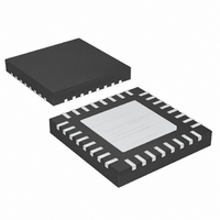
MAX17528GTJ+ Maxim Integrated Products, MAX17528GTJ+ Datasheet - Page 40

MAX17528GTJ+
Manufacturer Part Number
MAX17528GTJ+
Description
IC PWM CTRLR STP-DWN 32TQFN-EP
Manufacturer
Maxim Integrated Products
Series
Quick-PWM™r
Datasheet
1.MAX17528GTJ.pdf
(41 pages)
Specifications of MAX17528GTJ+
Applications
Controller, Intel IMVP-6.5™ GMCH
Voltage - Input
4.5 ~ 5.5 V
Number Of Outputs
1
Voltage - Output
0.01 ~ 1.5 V
Operating Temperature
-40°C ~ 105°C
Mounting Type
Surface Mount
Package / Case
32-TQFN Exposed Pad
Lead Free Status / RoHS Status
Lead free / RoHS Compliant
1-Phase Quick-PWM
Intel IMVP-6.5/GMCH Controllers
Careful PCB layout is critical to achieve low switching
losses and clean, stable operation. The switching
power stage requires particular attention. If possible,
mount all the power components on the top side of the
board with their ground terminals flush against one
another. Follow the MAX17528 Evaluation Kit layout and
use the following guidelines for good PCB layout:
•
•
•
•
•
40
High-current path/components: Keep the high-cur-
rent paths short, especially at the ground terminals.
This is essential for stable, jitter-free operation.
Keep the power traces and load connections short.
This is essential for high efficiency. The use of thick
copper PCBs (2oz vs. 1oz) can enhance full-load
efficiency by 1% or more. Correctly routing PCB
traces is a difficult task that must be approached in
terms of fractions of centimeters, where a single
mΩ of excess trace resistance causes a measur-
able efficiency penalty.
When trade-offs in trace lengths must be made, it is
preferable to allow the inductor charging path to be
made longer than the discharge path. For example,
it is better to allow some extra distance between the
input capacitors and the high-side MOSFET than to
allow distance between the inductor and the low-
side MOSFET or between the inductor and the out-
put filter capacitor.
MOSFET drivers: Keep the high-current, gate-dri-
ver traces (DL, DH, LX, and BST) short and wide
to minimize trace resistance and inductance. This
is essential for high-power MOSFETs that require
low-impedance gate drivers to avoid shoot-
through currents.
Analog control signals: Connect all analog grounds
to a separate solid copper plane, which connects to
the GND pin of the Quick-PWM controller as shown
in Figures 1 and 2. This includes the V
capacitor, remote-sense bypass capacitors, and
the compensation (CCV) components.
______________________________________________________________________________________
Applications Information
PCB Layout Guidelines
CC
bypass
•
•
1) Place the power components first, with ground ter-
2) Mount the controller IC adjacent to the low-side
3) Group the gate-drive components (BST capacitor,
4) Make the DC-DC controller ground connections as
5) Connect the output power planes (V
CSP and CSN connections for current limiting and
voltage positioning must be made using Kelvin-
sense connections to guarantee the current-sense
accuracy.
Route high-speed switching nodes (LX, DH, BST,
and DL) away from sensitive analog areas (FB,
CSP, CSN, CCV, etc.).
minals adjacent (low-side MOSFET source, C
C
connections on the top layer with wide, copper-
filled areas.
MOSFET. The DL gate traces must be short and
wide (50 mils to 100 mils wide if the MOSFET is 1in
from the controller IC).
V
shown in the standard application circuits. This dia-
gram can be viewed as having three separate
ground planes: input/output system ground, where
all the high-power components go; the power
ground plane, where the PGND pin and V
bypass capacitor go; and the controller’s analog
ground plane where sensitive analog components,
the analog GND pin, and V
The analog GND plane must meet the PGND plane
only at a single point directly beneath the controller.
This star ground point (where the power and analog
grounds are connected) should connect to the
high-power system ground with a low-impedance
connection (short trace or multiple vias) from PGND
to the source of the low-side MOSFET.
tem ground planes) directly to the output filter
capacitor positive and negative terminals with multi-
ple vias. Place the entire DC-DC converter circuit
as close as is practical to the CPU.
DD
OUT
bypass capacitor) together near the controller IC.
, and D1 anode). If possible, make all these
CC
Layout Procedure
bypass capacitor go.
CORE
and sys-
DD
IN
,


