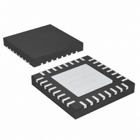
MAX17528GTJ+ Maxim Integrated Products, MAX17528GTJ+ Datasheet - Page 23

MAX17528GTJ+
Manufacturer Part Number
MAX17528GTJ+
Description
IC PWM CTRLR STP-DWN 32TQFN-EP
Manufacturer
Maxim Integrated Products
Series
Quick-PWM™r
Datasheet
1.MAX17528GTJ.pdf
(41 pages)
Specifications of MAX17528GTJ+
Applications
Controller, Intel IMVP-6.5™ GMCH
Voltage - Input
4.5 ~ 5.5 V
Number Of Outputs
1
Voltage - Output
0.01 ~ 1.5 V
Operating Temperature
-40°C ~ 105°C
Mounting Type
Surface Mount
Package / Case
32-TQFN Exposed Pad
Lead Free Status / RoHS Status
Lead free / RoHS Compliant
On-times translate only roughly to switching frequen-
cies. The on-times guaranteed in the Electrical
Characteristics table are influenced by switching
delays in the external high-side MOSFET. Resistive
losses, including the inductor, both MOSFETs, and
printed-circuit board (PCB) copper losses in the output
and ground tend to raise the switching frequency as
the load current increases. Under light-load conditions,
the dead-time effect increases the effective on-time,
reducing the switching frequency. It occurs only during
forced-PWM operation and dynamic output-voltage
transitions when the inductor current reverses at light-
or negative-load currents. With reversed inductor cur-
rent, the inductor’s EMF causes LX to go high earlier
than normal, extending the on-time by a period equal to
the DH-rising dead time. For loads above the critical
conduction point, where the dead-time effect is no
longer a factor, the actual switching frequency is:
where V
the inductor discharge path, including synchronous rec-
tifier, inductor, and PCB resistances; V
the parasitic voltage drops in the inductor charge path,
including high-side switch, inductor, and PCB resis-
tances; and t
The output current is differentially sensed by the high-
impedance current-sense inputs (CSP and CSN). Low-
offset amplifiers are used for voltage-positioning gain,
current-limit protection, and current monitoring. Sensing
the current at the output offers advantages, including less
noise sensitivity and the flexibility to use either a current-
sense resistor or the DC resistance of the power inductor.
Using the DC resistance (R
higher efficiency. In this configuration, the initial toler-
ance and temperature coefficient of the inductor’s DCR
must be accounted for in the output-voltage droop-
error budget and current monitor. This current-sense
method uses an RC filtering network to extract the cur-
rent information from the inductor (see Figure 4). The
resistive divider used should provide a current-sense
resistance (R
DIS
is the sum of the parasitic voltage drops in
ON
f
CS
SW
) low enough to meet the current-limit
is the on-time as determined above.
=
______________________________________________________________________________________
t
ON IN
(
V
(
V
OUT
+
DCR
V
DIS
+
) of the inductor allows
V
DIS
−
V
)
CHG
Current Sense
Intel IMVP-6.5/GMCH Controllers
CHG
)
is the sum of
requirements (R
constant of the RC network should match the inductor’s
time constant (L/R
and:
where R
R
worst-case inductance and R
the inductor manufacturer, adding some margin for the
inductance drop over temperature and load. To mini-
mize the current-sense error due to the current-sense
inputs’ bias current (I
than 2kΩ and use the above equation to determine the
sense capacitance (C
tolerance and resistors with 1% tolerance specifications.
Temperature compensation is recommended for this
current-sense method. See the Voltage Positioning and
Loop Compensation section for detailed information.
When using a current-sense resistor for accurate output-
voltage positioning, the circuit requires a differential RC
filter to eliminate the AC voltage step caused by the
equivalent series inductance (L
resistor (see Figure 4). The ESL-induced voltage step
does not affect the average current-sense voltage, but
results in a significant peak current-sense voltage error
that results in unwanted offsets in the regulation voltage
and results in early current-limit detection. Similar to the
inductor DCR sensing method, the RC filter’s time con-
stant should match the L/R time constant formed by the
current-sense resistor’s parasitic inductance:
where L
current-sense resistor, R
resistance value, C
matching components.
DCR
is the inductor’s series DC resistance. Use the
1-Phase Quick-PWM
CS
ESL
is the required current-sense resistance, and
is the equivalent series inductance of the
CS
R
R
DCR
DCR
CS
R
x I
EQ
L
SENSE
=
CSP
):
ESL
OUT(MAX)
EQ
=
⎛
⎜
⎝
and R1 are the time-constant
C
R
). Choose capacitors with 5%
), choose R1 || R2 to be less
1
L
EQ
R
SENSE
+
2
=
R
⎡
⎢
⎣
C
2
R
DCR
ESL
1
EQ
⎞
⎟
⎠
1
< 50mV), and the time
R
+
DCR
R
is the current-sense
) of the current-sense
R
1
values provided by
1
2
⎤
⎥
⎦
23


