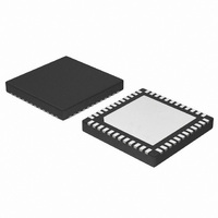
NCP4208MNR2G ON Semiconductor, NCP4208MNR2G Datasheet - Page 16

NCP4208MNR2G
Manufacturer Part Number
NCP4208MNR2G
Description
IC CTLR 8PH VR11.1 PMBUS 48-QFN
Manufacturer
ON Semiconductor
Datasheet
1.NCP4208MNR2G.pdf
(30 pages)
Specifications of NCP4208MNR2G
Applications
Controller, Intel VR11.1
Voltage - Input
4.7 ~ 5.75 V
Number Of Outputs
8
Voltage - Output
0.16 ~ 5 V
Operating Temperature
0°C ~ 85°C
Mounting Type
Surface Mount
Package / Case
48-TQFN Exposed Pad
Output Voltage
0.375 V to 1.6 V
Input Voltage
0.3 V to 6 V
Switching Frequency
1.5 MHz
Operating Temperature Range
0 C to + 85 C
Mounting Style
SMD/SMT
Duty Cycle (max)
100 %
Lead Free Status / RoHS Status
Lead free / RoHS Compliant
Available stocks
Company
Part Number
Manufacturer
Quantity
Price
Company:
Part Number:
NCP4208MNR2G
Manufacturer:
ON Semiconductor
Quantity:
1 200
Part Number:
NCP4208MNR2G
Manufacturer:
ON/安森美
Quantity:
20 000
I
Interface. The NCP4208 SMBus address is 0x20
(010 0000). With the R/W bit set to 0 this gives an 8 bit
address of 0x40.
pulses: 8 bits of data followed by an acknowledge bit from
the slave device. Transitions on the data line must occur
during the low period of the clock signal and remain stable
during the high period, because a low−to−high transition
when the clock is high might be interpreted as a stop signal.
The number of data bytes that can be transmitted over the
serial bus in a single read or write operation is limited only
by what the master and slave devices can handle.
2
C Interface
Control of the NCP4208 is carried out using the I
Data is sent over the serial bus in sequences of nine clock
1. When all data bytes have been read or written, stop
START BY MASTER
conditions are established. In write mode, the
master pulls the data line high during the tenth
clock pulse to assert a stop condition. In read mode,
the master device overrides the acknowledge bit by
pulling the data line high during the low period
before the ninth clock pulse; this is known as No
Acknowledge. The master takes the data line low
during the low period before the tenth clock pulse,
and then high during the tenth clock pulse to assert
a stop condition.
Any number of bytes of data can be transferred over
the serial bus in one operation, but it is not possible
to mix read and write in one operation because the
type of operation is determined at the beginning and
cannot subsequently be changed without starting a
new operation.
In the NCP4208, write operations contain one, two
or three bytes, and read operations contain one or
SDA
SCL
SDA
SCL
START BY
MASTER
1
0
1
1
0
1
0
SERIAL BUS ADDRESS
0
0
FRAME 1
SERIAL BUS ADDRESS
BYTE
0
0
FRAME 1
BYTE
0
0
SDA (CONTINUED)
SCL (CONTINUED)
Figure 12. Write Byte
Figure 11. Send Byte
http://onsemi.com
0
0
ACK. BY NCP4208
2
C
R/W
0
16
R/W
9
ACK. BY
NCP4208
D7
9
1
D7
1
2. The read byte operation is shown in Figure 13. First
the command code needs to be written to the
NCP4208 so that the required data is sent back.
This is done by performing a write to the NCP4208
as before, but only the data byte containing the
register address is sent, because no data is written to
the register. A repeated start is then issued and a
read operation is then performed consisting of the
serial bus address; R/
data byte read from the data register.
two bytes. The command code or register address
determines the number of bytes to be read or written,
See the register map for more information.
To write data to one of the device data registers or
read data from it, the address pointer register must
be set so that the correct data register is addressed
(i.e. command code), and then data can be written to
that register or read from it. The first byte of a read
or write operation always contains an address that is
stored in the address pointer register. If data is to be
written to the device, the write operation contains a
second data byte that is written to the register
selected by the address pointer register.
This write byte operation is shown in Figure 12. The
device address is sent over the bus, and then R/
set to 0. This is followed by two data bytes. The first
data byte is the address of the internal data register
to be written to, which is stored in the address
pointer register. The second data byte is the data to
be written to the internal data register.
D6
D7
1
D6
D6
D5
D5
D4
D5
D4
COMMAND CODE
FRAME 3
FRAME 2
D4
D ATA
BYTE
COMMAND CODE
D3
D3
FRAME 2
W
D3
D2
D2
bit set to 1, followed by the
D1
D2
D1
ACK. BY NCP4208
D0
D1
D0
NCP4208
ACK. BY
D0
9
9
NCP4208
ACK. BY
9
STOP BY
MASTER
STOP BY
MASTER
W
is


